
2. Impurities in Semiconductors
- Page ID
- 5954
| Contents |
Group 3 and 5 Dopants
When foreign atoms are introduced into a semiconductor material, the characteristics of the material change. Depending on whether the added impurities have “extra” electrons or “missing” electrons determines how the bonding in the crystal lattice is affected, and therefore how the material’s electrical properties change. By doping a semiconductor (by adding impurities to an intrinsic semiconductor, see Intrinsic Carrier Concentration), we can manipulate the equilibrium behavior of the material.
Group III dopants are atoms with a hole in their valence shell (only “missing” one electron) while Group V dopants are atoms with an “extra” electron, in other words a valence shell with only one electron. Group III elements can be found in the IIIA column of the Periodic Table, while Group V elements can be found in the VA column (hence the names). When a semiconductor is doped with a Group III impurity it is called a p-type material, because it now contains a surplus of positively “charged” holes. When a semiconductor is doped with a Group V impurity it is called an n-type material, because it now contains a surplus of negatively charged electrons not bonded to the surrounding semiconductor atoms. In an n-type semiconductor, the majority carrier, or the more abundant charge carrier, is the electron, and the minority carrier, or the less abundant charge carrier, is the hole.
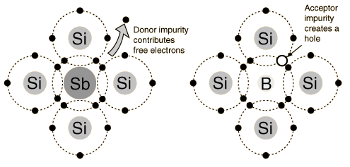
Above is an illustration of Silicon atoms with full shells of electrons bonded to an Antimony atom (Sb, left), and Silicon atoms bonded to a Boron atom (B, right). The Sb is a Group V dopant with an extra electron (donor) while Boron is a Group III dopant with an empty “space” (hole) for accepting electrons.
<hyperphysics.phy-astr.gsu.edu...lids/dope.html>
Charge Neutrality
Before we proceed, it is worth noting the importance of the overall charge of atoms in the material. As depicted above, Group V atoms have an “extra” electron (or one valence electron), and the atom is therefore considered a donor of electrons. This is so because the valence electron is so easily stripped from the atom for conduction, or to freely move in the material. This is a result of the electron wanting to move to where it is energetically favorable; it is more favorable to become conductive in a semiconductor at room temperature than it is to try to stay bound to its already “full” atom. Similarly, Group III atoms are considered acceptors because they more readily accept electrons than give up electrons.
This overall accepting or donating of electrons in P- and N-Type materials results in a net charge on the atom; there is no longer a neutrality maintained because there are not as many electrons in the impure atoms (including shared electrons) as there are protons in the nucleus. In other words, in a doped semiconductor, the ionized atoms will have a non-neutral charge depending on the material (P-Type or N-Type).
Of course, it is most useful to use the charge neutrality conditions inside the material to obtain the number of charge carriers in the doped material.
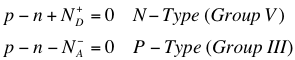
The above equations1 tells us that in an N-Type material (where there are Group V impurities present in the intrinsic semiconductor), because the extra electrons are mostly freed from the atom at room temperature, the positive charge left with the ionized atom must be included with the total charge density in the material. Similarly, the negative charge accumulated by atoms that have “accepted” excess electrons must be taken into account. It is worth noting here that majority carriers are free charge carriers because they are easily stripped from the atoms; this is a natural result of doping, and the carriers are introduced directly into the conduction band (if an electron) or valence band (if a hole).
References
1. Green, Martin A. Solar Cells: Operating Principles, Technology, and System Applications. Englewood Cliffs: Prentice-Hall, Inc., 1982. Full book ordering information at www.pv.unsw.edu.au.