
19.1: Introduction
- Page ID
- 35886

To fully appreciate the software interface to microcontrollers and to gain insight into how to interface controllers to external devices, it is useful to examine the underlying circuitry. In this chapter we shall investigate the basic digital output circuitry. Anything that can be controlled with a simple logical yes/no, true/false input can be a target. Although controllers usually have limited output current and voltage capability, they can control devices such as power transistors which can in turn control more demanding loads. A simplified diagram of the General Purpose Input-Output (GPIO) circuitry can be seen in Figure \(\PageIndex{1}\).
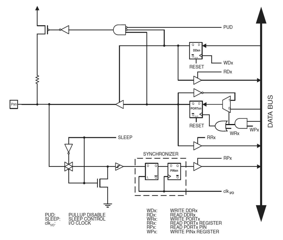
The circuit represents a single bit. An IO port consists of eight bits, typically. Therefore this circuitry would be replicated seven more times to accommodate a single byte-wide port, of which there may be several. Also, in order to reduce the external pin count of the IC, pins may be multiplexed with other functions. The multiplexers are not shown in this schematic. Pxn, at the far left of the schematic, represents the physical output pin. The data bus shown along the right edge is the source for data being written to the physical pin and also the destination for data being read from the pin. For now we shall focus on writing to the output and examine input functionality in a later chapter. While this circuit is specific to the ATmega series, it is representative of GPIO circuitry found in many microcontrollers.