
20.2: Input Circuitry
- Page ID
- 35890

Figure \(\PageIndex{1}\) presents a further simplification focusing solely on the input portion.
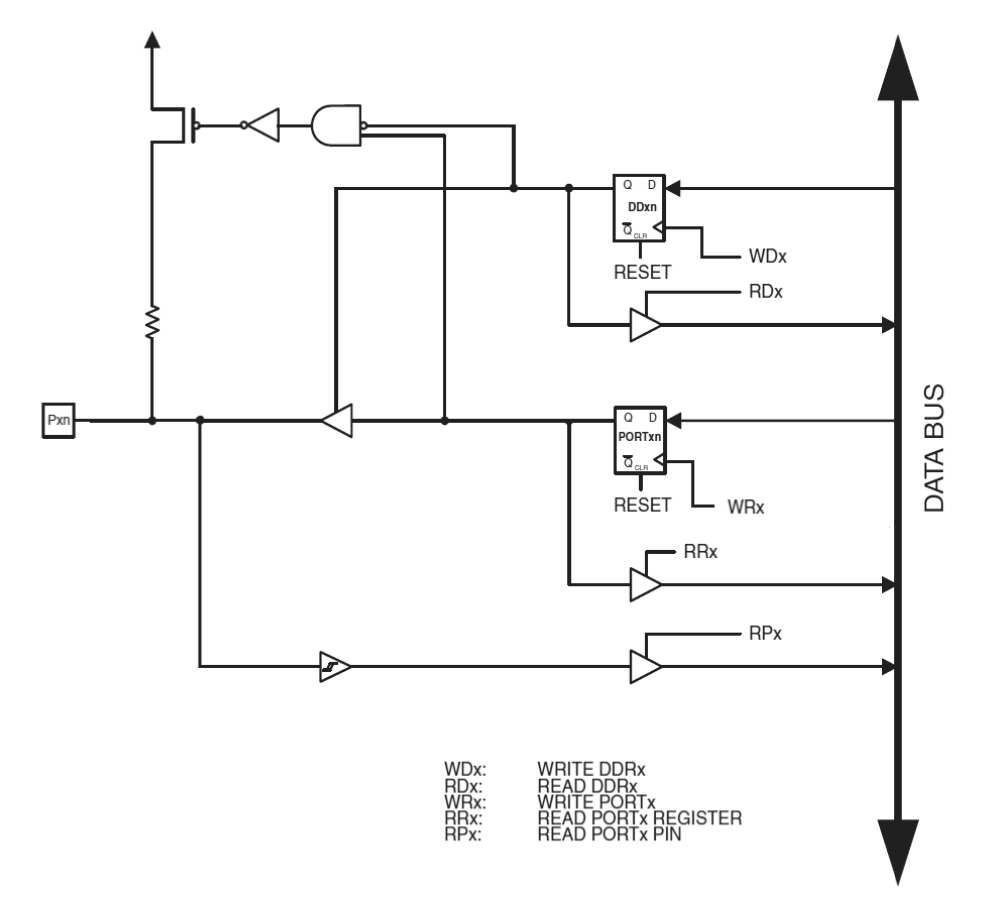
Once again we have removed the gates surrounding PORTxn that create the bit toggle function. Further, we have removed the PUD, SLEEP and CLK signals and simplified the lower section leaving just the Schmitt Trigger. The read process will be similar to the write process examined in the previous chapter.
To read a signal on an external pin, we will need to write a logic low to the data direction bit DDxn. This will disconnect PORTxn from the physical pin, Pxn, because the tri-state buffer will go to high-Z state. If PORTxn was left connected, the external device would wind up trying to drive the active output of PORTxn. This would produce unpredictable results at best.
Now that PORTxn is disconnected from Pxn, the signal existing at Pxn drives the Schmitt Trigger located along the bottom edge of the diagram. This signal will be passed on to the data bus once the RPx (Read Pin x) control signal is asserted on the lower tri-state buffer. A Schmitt Trigger is used as an intermediary here as we cannot be certain of clean, noise-free input signals. Also, note that the input signals are read from a PIN register (e.g., PINB or PINC). This is in contrast to the PORT registers used when writing data. Thus, if you want to write data to the outside world, you write to a PORT register. If you want to read data from the outside world, you read from a PIN register. Not all microcontrollers use this naming convention. Some use a single PORT register for both writing and reading. A good mnemonic for remembering whether PIN or PORT is used for input or output is to associate the “in” in PIN and the “o” (for output) in PORT. Typically, the PORT, PIN and DDR registers are adjacent in the memory map. For example, using port B we find PINB at 0x23, DDRB at 0x24 and PORTB at 0x25. Check the register map in the Appendix for more.
We are still left with the MOSFET section. This is used to generate an optional pull-up resistor. There are two basic ways to generate input signals. The first is with an active circuit. For example, the output of a logic gate could be connected to the external pin. The voltage produced by the gate would be fed to the Schmitt Trigger as described previously and the signal would make its way to the data bus. It is not always convenient to generate an external voltage with an active circuit, though. If you wanted to read the state of a simple push button, you couldn’t just connect it between the pin and ground as there would be no signal to sense. Instead you’d have to connect it to an external power supply through a limiting resistor, requiring more components and space. The pull-up takes care of this for you. When activated, the MOSFET connects its associated resistor to the internal power line. If a switch is now connected between the external pin and ground, and is closed, the pin is pulled to ground (i.e., logic low). If the switch is opened, the resistor “pulls up” the pin voltage to the supply rail (i.e., logic high). Thus, we can determine the state of the switch with no other external circuitry.
To activate the pull-up, first the pin must be in input mode (DDxn at logic low which feeds the AND gate). Also, the output of PORTxn must be logic high. These two signals will drive the AND gate’s output high, turning on the MOSFET and engaging the pull-up resistor. It might seem a little odd to be writing to the PORT bit for read mode but this is just a neat way of making the most of the available hardware. After all, in read mode, the PORT register is otherwise unused. Why let it go to waste and require yet another register to control the pull-up?
In summary, to read from the external pin, a low is written to the appropriate DDR bit, placing this circuit in read (input) mode. If a pull-up is desired, a high is written to the appropriate PORT bit. If a pull-up is not desired, a low is written to the PORT bit. Once this is done, the external value can be read from the PIN register. As with the output circuitry, the DDR and PORT do not have to be rewritten prior to each subsequent read from the PIN. The D flip-flops will hold their values until they are rewritten, thus maintaining the current data direction and pull-up status.