4.5: Implementing the AND Gate Circuit
- Page ID
- 26971

This section will cover how to implement the AND gate circuit. This circuit will add a new component to the circuit, a 7408 (AND) chip to implement the AND gate. A brief overview of the 7408 chip will be given here.
\(\PageIndex{1}\) ICs and the 7408 chip
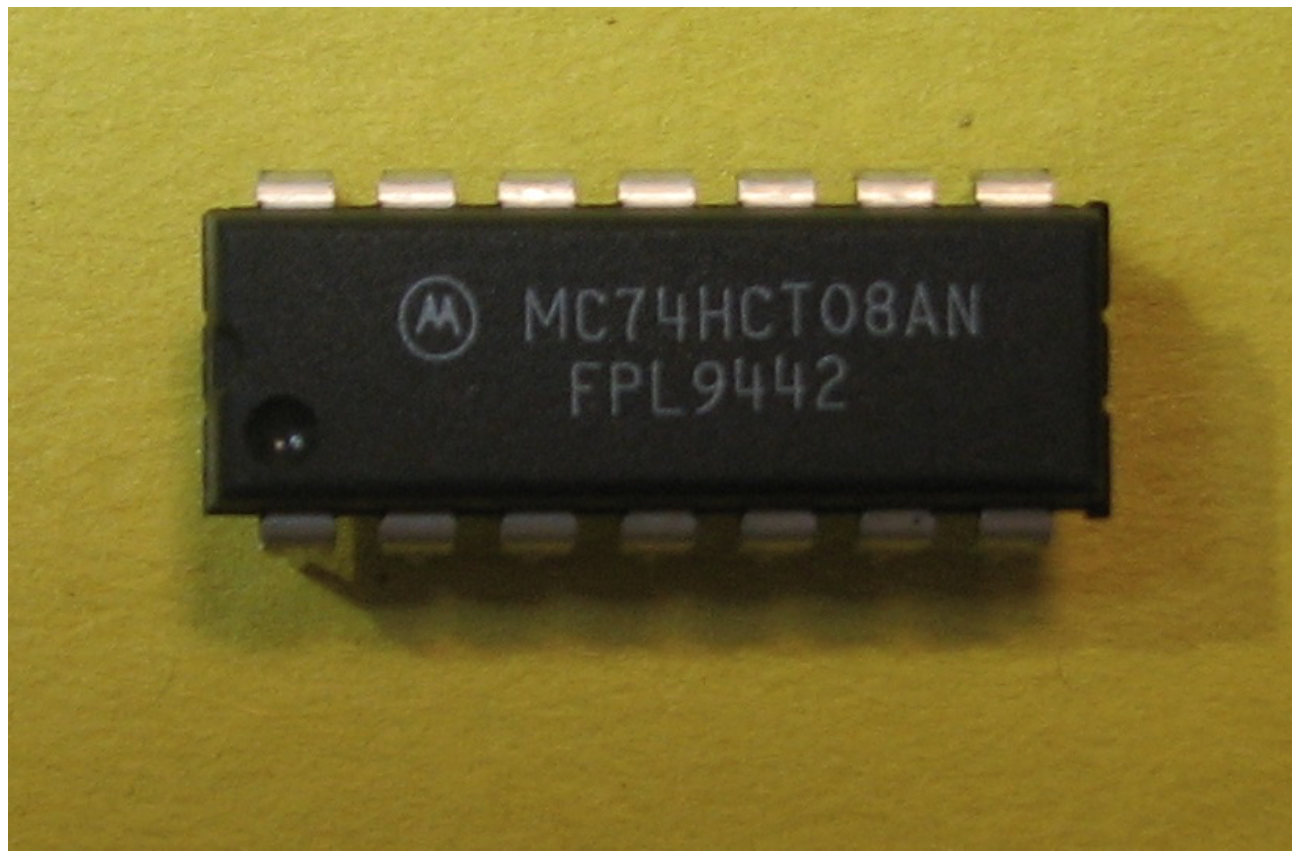
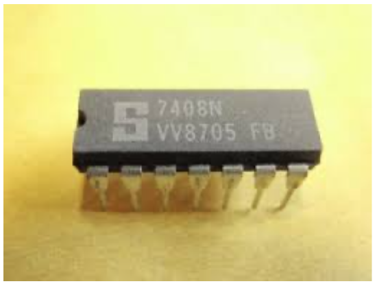
Figures \(\PageIndex{1}\) and \(\PageIndex{2}\) are pictures of 7408 chips. There are a large number of manufactures of chips, and realtors will usually sell chips from several different manufactures. While the chips themselves are standard in their implementation and packaging, details such as the labeling are not. All chips are labeled on the top of the chip, though the labeling is not consistent. Some labels are easy to read, but often the labels require the user to move the chip around under a bright light to see the labeling. Other types of manufacturer specific information will be on the chip, and this will vary from manufacturer to manufacturer. But somewhere on the chip will be a designation of the chip type. This designation will follow the format of 74tttsss, as explained in section 1.2.
Every chip some number of sharp legs, called pins, which are designed to be inserted into the breadboard. Each pin has a specific use. For the 7408 chip these pins will be explained in the next section. Be careful when inserting and removing these chips, as these pins are delicate and easily bend and break.
\(\PageIndex{2}\) The datasheet
Every IC chip comes with a datasheet which explains the setup of the chip. The datasheet contains a lot of useful information to engineers looking to use these chips, much of it beyond the scope of this text. One diagram that is always available in the datasheet is the pin configuration, and example for the 7408 chip shown in Figure \(\PageIndex{3}\) below.
The pin configuration diagram contains several items. The first is the orientation of the chip. At the top of every chip is a circle or notch, shown in Figures \(\PageIndex{1}\) and \(\PageIndex{2}\) respectively. It is important to carefully note the top of the chip, as inserting the chip upside down is a common mistake. When this happens, generally the VCC and GND wires are reversed, and the chip becomes hot very quickly. It is always a good idea to check the powering of the chip when it is placed on the board to make sure it is not getting hot.
Next the pin configuration diagram shows the input and output values for the pins on the chip. As shown in Figure \(\PageIndex{3}\), there are 4 AND gates on this chip. Pins 1 and 2 are inputs to an AND gate which has output on pin 3. Likewise pins 4 and 5 connect to pin 6, etc.
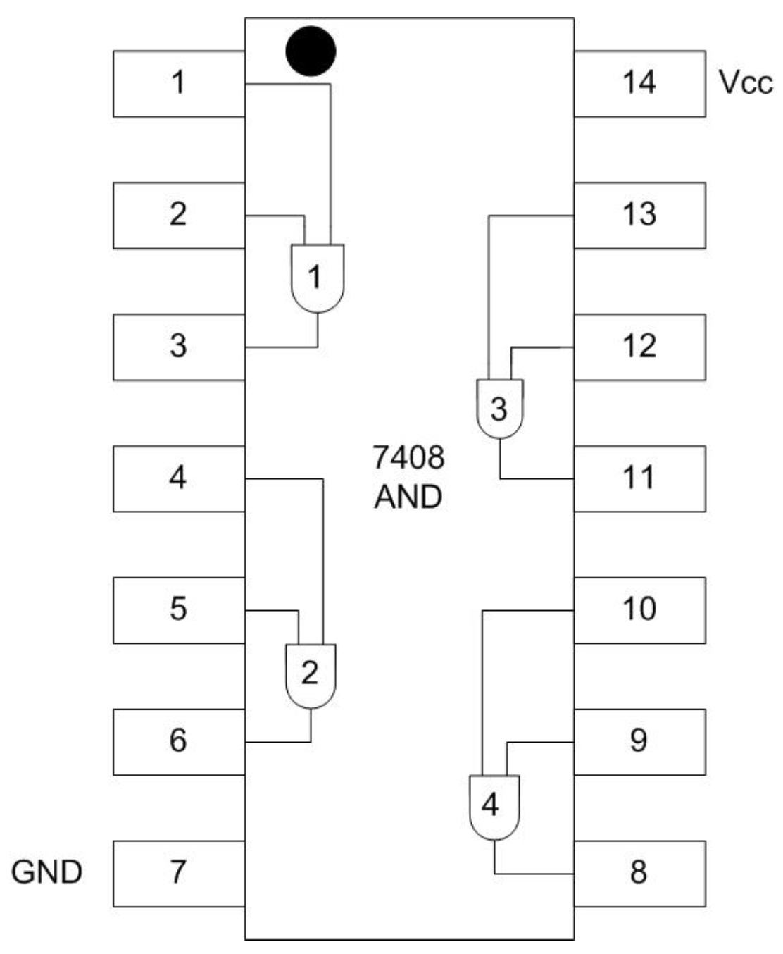
There are two pins which are not connected to any gates, labeled VCC and GND. All chips must be powered to work. The VCC and GND are known as the power supply pins. These are the pins which are connected to the positive and negative rails to provide power to the circuit. As can be seen in Figure \(\PageIndex{4}\) the VCC (pin 14) is connected to the positive (red) rail using a red wire, and GND (pin 7) is connected to the ground (blue) rail using a black wire.
We are now ready to implement the circuit to implement a single AND gate to turn on a LED.
\(\PageIndex{3}\) Creating the AND circuit
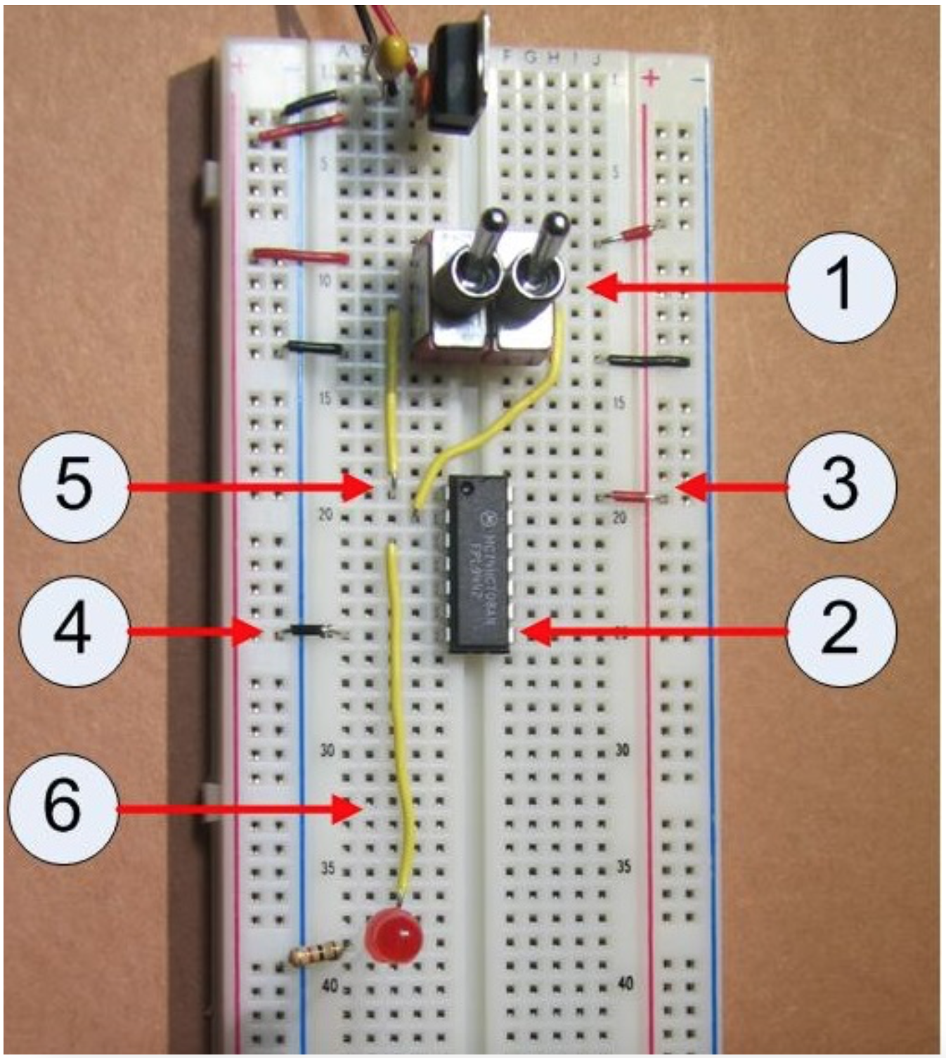
This section covers how to implement a circuit using an AND chip. The steps correspond to the picture in Figure \(\PageIndex{4}\).
- Insert a second switch on the right hand side of the breadboard, and wire it just like the switch installed in Chapter 3. The right hand side of the breadboard should have been powered as part of the original circuit in Chapter 3.
- Carefully insert the 7408 (AND gate) chip onto the breadboard, being careful not to bend the pins on the chip. The chip is placed so that it crosses the middle of the board. Make sure that the circle or notch is at the top of the circuit, as in Figure \(\PageIndex{4}\).
- Provide power to the chip by connecting pin 14 to the positive rail.
- Ground the chip by connecting pin 7 to the ground rail.
- Connect the input pins 1 and 2 to the inputs from the two switches.
- Connect the output pin 3 to the LED.
If everything is connected correctly, the circuit will implement an AND gate with the input coming from the two switches.