
4.2: The Bipolar Junction Transistor
- Page ID
- 25405

In prior work we discovered that the PN junction is the foundation of the basic diode. Under normal operating conditions the interface between the N-type and P-type materials is devoid of free charges and is referred to as a depletion region. The dissimilar Fermi levels of N-type and P-type materials lead to an “energy hill” between them, and without an external potential of the proper polarity, the junction will not allow current to flow. The required magnitude is a function of the material used but it is always the case that the P material (anode) must be positive with respect to the N material (anode). We extend this idea by adding a second portion of N material to the other side of the P material, creating an N-P-N “sandwich” of sorts. This is shown in Figure \(\PageIndex{1}\).
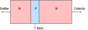
Figure \(\PageIndex{1}\): Basic configuration of NPN bipolar junction transistor.
This diagram is drawn to ease the understanding of the operation of the device, extending our earlier diode work. In contrast, real BJTs are built in more of a “layer cake” fashion, N-P-N bottom to top1. Of course, the spatial orientation of the device has no bearing on its operation so this is not a major issue for our purposes. The three terminals are named the emitter, base and collector. The collector is the largest of the three regions while the base is relatively thin and lightly doped.
Above absolute zero there will be recombination and two depletion regions will form as shown in Figure \(\PageIndex{2}\). Compare this figure to the basic PN junction drawing found at the beginning of Chapter 2, Figure 2.1.1.
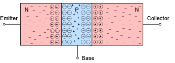
Figure \(\PageIndex{2}\): Charges in NPN BJT (base region widened to show detail).
4.2.1: A Simple Two-Diode Model
Because this device contains two depletion regions, a much simplified model can be created using two diodes as shown in Figure \(\PageIndex{3}\). Please keep in mind that this is a very limited model (as we shall soon see).
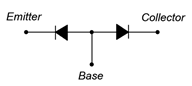
Figure \(\PageIndex{3}\): Diode model of NPN BJT.
If you were to test an NPN BJT with an ohmmeter, two leads at time, this model would successfully predict the results. If the red (positive) lead of the ohmmeter is connected to the base and the black (negative) lead is connected to either the emitter or collector, a low resistance will be indicated. This is because the ohmmeter will modestly forward-bias the base-emitter or base-collector junction. Similarly, if the leads are reversed, the meter will indicate high resistance because the junction under consideration will be reverse-biased. If the two leads are connected to the emitter and collector, a high reading will result regardless of the polarity. This is because one of the two junctions will be reverse-biased which results in no current flow through either of them due to the series connection.
4.2.2: Biasing the BJT
Now let's consider adding external sources to bias the transistor. We begin by adding two DC sources with associated current limiting resistors as shown in Figure \(\PageIndex{4}\).
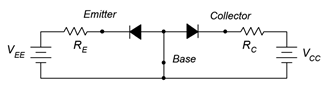
Figure \(\PageIndex{4}\): Double reverse-bias.
This circuit is comprised of two loops, one between the base-emitter and the second between the base-collector. In the B-E loop, the emitter supply \(V_{EE}\) reverse-biases the base-emitter diode. A similar situation occurs in B-C loop where the collector supply reverse-biases the base-collector diode. The result is that virtually no current flows anywhere in the circuit. If the two supplies are reversed in polarity then both diodes become forward-biased and we see currents flowing in both loops dependent on the precise values of the supplies and associated resistors. No surprises so far. Now consider if we forward-bias the base-emitter diode while simultaneously reversebiasing the base-collector diode, as shown in Figure \(\PageIndex{5}\).
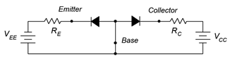
Figure \(\PageIndex{5}\): Forward-reverse bias.
With a simple pair of diodes we'd expect the B-E loop to show a high current and the B-C loop show negligible current. With a BJT, this is not what happens. Instead, what we see is a high current in both loops, and those currents are very nearly equal in magnitude. How does this come about?
The key to understanding this situation is that the base of the BJT is thin and lightly doped. In contrast, the dual diode model splits the base into two separate pieces of material and that makes all the difference. To get a better handle on what's happening here, let's take a closer look at this forward-reverse bias circuit but this time substituting the transistor diagram of Figure \(\PageIndex{2}\). Refer to Figure \(\PageIndex{6}\).
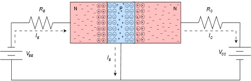
Figure \(\PageIndex{6}\): Forward-reverse bias, electron flow.
Electron flow will facilitate this explanation so we'll draw the current directions using dashed lines. From the left side of the diagram, electrons exit the emitter supply and enter the N emitter. Here they are the majority carrier. The base-emitter depletion creates an energy hill just as it did with a single PN junction. As long as there is sufficient potential from the emitter supply, the electrons will be pushed into the base. These electrons will attempt to recombine with the majority base holes, however, because the base is physically thin and lightly doped, only a small percentage of the injected electrons will recombine with base holes and exit the base terminal back to ground. This current is called the base current current or the recombination current. Meanwhile, the vast majority of the remaining electrons (95% to over 99%) will find their way to the base-collector depletion region and then to the collector. Once in the collector, the electrons are again the majority carrier and flow back to the positive terminal of the collector power supply. The energy diagram of the transistor is depicted in Figure \(\PageIndex{7}\). Compare this to the single PN junction energy diagram found at the beginning of Chapter 2, Figure 2.1.2.
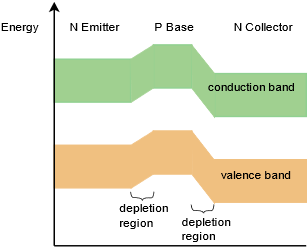
Figure \(\PageIndex{7}\): Energy diagram of BJT.
At first glance, it might appear as though the emitter and collector leads can be swapped with no change in operation. With real-world devices this is not possible generally because the emitter and collector regions are optimized and not physically identical. Thus, placing transistors into a circuit backwards, with emitter and collector leads swapped, will usually result in unpredictable behavior.
Based on the foregoing discussion and what we already know about PN junctions, we can summarize transistor performance as follows:
- From KCL, \(I_E = I_C + I_B\).
- \(I_C \gg I_B\), therefore \(I_E \approx I_C\).
- The base-emitter junction is forward-biased, therefore \(V_{BE} \approx 0.7\) V (silicon).
- The base-collector junction is reverse-biased, therefore \(V_{CB}\) is large.
- Conventional current flows into the collector and base, and out of the emitter.
We can also define a couple of transistor performance parameters. The ratio of collector current to emitter current is called \(\alpha \) (alpha). \(\alpha \) typically is greater than 0.95. A somewhat more useful parameter is the ratio of collector current to base current. This is called \(\beta \) (beta) and can also be found on transistor spec sheets as \(h_{FE}\) (\(h_{FE}\) is one of four hybrid parameters). It is also referred to generically as current gain (if \(I_B\) is in the input signal and \(I_C\) is the output signal then \(\beta \) represents the amount of signal boost or gain). For small signal transistors \(\beta \) typically is in the range of 100 to 200, although it can be larger. For power transistors, \(\beta \) tends to be smaller, more like 25 to 50. Presented as formulas we have:
\[\alpha = I_C / I_E \label{4.1} \]
\[\beta = I_C / I_B \label{4.2} \]
And with a little math,
\[\alpha = \beta / (\beta +1) \nonumber \]
\[\beta = \alpha / (1−\alpha ) \nonumber \]
\[I_C = \beta I_B \nonumber \]
Finally, we come to the schematic symbol of the NPN BJT, as shown in Figure \(\PageIndex{8}\). A common variation places the body of the device within a circle. Following the standard, the arrow points to N material and in the direction of easy conventional current flow.
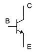
Figure \(\PageIndex{8}\): NPN Schematic symbol
4.2.3: The PNP Bipolar Junction Transistor
The PNP version of the BJT is created by swapping the material for each layer. The outcome is the logical inverse of the NPN regarding current directions and voltage polarities. That is, conventional current flows into the emitter, and out of the collector and base (echoing the electron flow of the NPN). Further, voltages across the device have reversed polarity, for example, \(V_{BE} \approx −0.7\) V. All of the other characteristics remain unchanged so equations such \ref{4.1} and \ref{4.2} are still applicable. Just about any NPN-based circuit has its PNP counterpart. The schematic symbol of the PNP reverses the emitter arrow. As the base is now the N material, the arrow points toward the base. This is illustrated in Figure \(\PageIndex{9}\).
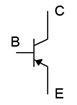
Figure \(\PageIndex{9}\): PNP Schematic symbol
References
1Homer says, “Mmm, NPN layer cake sandwich...”