
4.6: DC Load Lines
- Page ID
- 25409

So how do we determine the range of possible values of collector current and collector-emitter voltage in any given DC BJT circuit? One answer is to employ the concept of the DC load line. In general, a load line is a plot of all possible coordinate pairs of \(I_C\) and \(V_{CE}\) for a transistor in a given circuit. Referring back to Figure 4.5.3, we pick up with Equation 4.5.2 and solve it for \(I_C\):
\[V_{CE} = V_{CC} −I_C R_C \\ I_C = \frac{1}{R_C} (V_{CC} −V_{CE} ) \\ I_C = − \frac{1}{R_C} V_{CE} + \frac{V_{CC}}{R_C} \label{4.5} \]
Equation \ref{4.5} is a linear equation of the form \(y = mx + b\). The y intercept (the value of \(I_C\) when \(V_{CE} = 0\)) is \(V_{CC}/R_C\). This is the maximum collector current that can be achieved. At this point the transistor is saturated and this maximum is referred to as \(I_{C(sat)}\). The x intercept (the value of \(V_{CE}\) when \(I_C = 0\)) is \(V_{CC}\). This represents the largest possible voltage across the transistor's collector-emitter. At this point the current is cut off, and therefore this voltage is called \(V_{CE(cutoff)}\). Lastly, the slope of the line is \(−1/R_C\). A plot is shown in Figure \(\PageIndex{1}\).
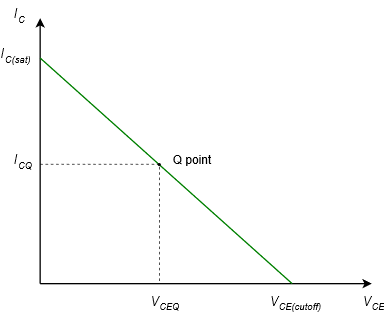
Figure \(\PageIndex{1}\): Generic DC load line.
To complete the graph, we also include the operating point for some specific transistor. This is called the quiescent point, or Q point, and the associated device current and voltage are called \(I_{CQ}\) and \(V_{CEQ}\). All possible Q points lay on this line.
Referring back to Example 4.5.1 and using Equation \ref{4.5}, we can summarize the circuit as follows:
\[I_{C(sat)} = 15 mA \\ V_{CE(cutoff)} = 15 V \nonumber \]
\[\text{Q Point for } \beta = 100: \\ I_C = 4.65 mA \\ V_{CE} = 10.35 V \nonumber \]
\[\text{Q Point for } \beta = 200: \\ I_C = 9.3 mA \\ V_{CE} = 5.7 V \nonumber \]
This is plotted in Figure \(\PageIndex{2}\).
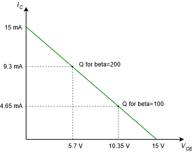
Figure \(\PageIndex{2}\): Load line for the variations on Example 4.5.1.
If we calculate a collector current that is greater than the saturation current, then we know that the actual current will be the saturation current maximum. For this circuit, any calculated value greater than 15 mA indicates that the transistor would produce only 15 mA (our earlier example using \(\beta\) = 400, for instance). In reality, the true value will be very slightly less. This is because the collector-emitter voltage does not go all the way down to zero volts when the device is saturated. Typically, \(V_{CE(sat)}\) will be a tenth of a volt or so for small signal devices. Precise values can be determined from device graphs such as the middle graph of Figure 4.4.1c, labeled “Collector Saturation Region”. As an example, if \(I_C\) = 10 mA and \(I_B\) = 0.3 mA, then \(V_{CE(SAT)}\) is approximately 0.15 V. It turns out that we can use saturation to our advantage in switching circuits, as we are about see.