
5.3: Two-Supply Emitter Bias
- Page ID
- 25413

For proper functioning, the collector-base junction needs to be reverse-biased and the base-emitter junction needs to be forward-biased. For an NPN transistor that means that the collector must be at the highest potential, the base somewhat lower and the emitter at the lowest potential of the three. One way of doing this is to apply the usual positive supply to the collector, but instead of using a second potential at the base, the base is tied to ground through a resistor. The requisite forward-bias on the base-emitter is then achieved by connecting the emitter to a negative power supply. This circuit configuration is shown in Figure \(\PageIndex{1}\) using an NPN device. We shall refer to this as two-supply emitter bias.
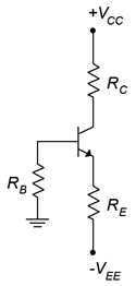
Figure \(\PageIndex{1}\): Two-supply emitter bias, NPN version.
We can derive an equation for the collector current by applying KVL to the baseemitter loop:
\[V_{EE} = V_{R_B} +V_{BE}+V_{R_E} \nonumber \]
\[V_{EE} = I_B R_B+V_{BE}+I_E R_E \nonumber \]
Recalling that \(I_B = I_C/ \beta\) and \(I_E \approx I_C\),
\[V_{EE} = (I_C/ \beta )R_B+V_BE+ I_C R_E \nonumber \]
Solving for \(I_C\) we arrive at
\[I_C = \frac{∣V_{EE}∣−V_{BE}}{R_E+R_B / \beta} \label{5.1} \]
The absolute value has been added to the emitter supply voltage so there is no confusion regarding the sign of this potential in the equation.
The thing to notice about Equation \ref{5.1} is that \( \beta \) only partly determines the collector current. In fact, if we can make \(R_E \gg R_B/ \beta\), then the equation reduces to
\[I_C \approx \frac{∣V_{EE}∣−V_{BE}}{R_E} \label{5.2} \]
It is relatively easy to achieve the \(R_E \gg R_B/ \beta\) stipulation. Given typical values of \( \beta \), this will be the case if \(R_E\) is approximately equal to or larger than \(R_B\). What we find in this instance is that almost all of the emitter supply drops across \(R_E\) to establish a stable \(I_C\) with \( \beta \) playing virtually no role. If \( \beta \) changes, the result will be an inverse change in \(I_B\) with \(I_C\) remaining largely unchanged.
Now that we have the collector current, any other current or voltage in the circuit may be derived by applying Ohm's law, KVL and the like. For example, to find \(V_C\), the voltage from the collector to ground,
\[V_C = V_{CC} − V_{R_C} \nonumber \]
\[V_C = V_{CC} − I_C R_C \nonumber \]
And to find the transistor's collector-emitter voltage, \(V_{CE}\),
\[V_{CE} = V_{CC}+∣V_{EE}∣−V_{RC} −V_{RE} \\ V_{CE} = V_{CC}+∣V_{EE}∣−I_C R_C −I_C R_E \\ V_{CE} = V_{CC}+∣V_{EE}∣−I_C (R_C+R_E ) \label{5.3} \]
Note that \(V_{CE}\) can also be found via \(V_{CE} = V_C − V_E\). Dropping voltages along the base-emitter loop yields
\[V_E = −V_{R_B} −V_{BE} \nonumber \]
\[V_E = −I_B R_B −V_{BE} \nonumber \]
Also, it is to our advantage to develop the DC load line for this configuration. The load line can serve as a “sanity check” for our computations. To find the endpoints, \(I_{C(sat)}\) is the maximum current and will occur when \(V_{CE} = 0\). If we imagine the current rising as \(V_{CE}\) collapses, eventually all of the available supply voltage will have dropped across \(R_C\) and \(R_E\). Thus
\[I_{C(sat)} = \frac{V_{CC}+∣V_{EE}∣}{R_C+R_E} \label{5.4} \]
Similarly, \(V_{CE(cutoff)}\) occurs when \(I_C = 0\). That means that there will be no potentials across \(R_C\) and \(R_E\). Therefore, \(V_{CE}\) “absorbs” the entire available source voltage.
\[V_{CE (cutoff )} = V_{CC}+∣V_{EE} ∣ \label{5.5} \]
Do not attempt to memorize all of the myriad equations presented. There are simply too many variations on the theme and it will only get worse when other biasing configurations are introduced. Instead, remember how to find the collector current and then get in the habit of applying Ohm's law and KVL to derive whatever else you may need.
At this point a comprehensive example is called for.
Example \(\PageIndex{1}\)
Assuming \( \beta = 100\), plot the Q point (\(I_C\) and \(V_{CE}\)) on the load line for the circuit of Figure \(\PageIndex{2}\).
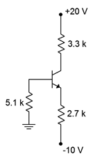
Figure \(\PageIndex{2}\): Circuit for Example \(\PageIndex{1}\).
Using Equation \ref{5.1}:
\[I_C = \frac{∣V_{EE} ∣−V_{BE}}{R_E+R_B / \beta} \nonumber \]
\[I_C = \frac{10 −0.7}{2.7k \Omega +5.1 k \Omega /100} \nonumber \]
\[I_C = 3.38 mA \nonumber \]
Noting the relative sizes of \(R_E\) and \(R_B\), the approximation should be close.
\[I_C = \frac{∣V_{EE} ∣−V_{BE}}{R_E} \nonumber \]
\[I_C = \frac{10 −0.7}{2.7 k \Omega} \nonumber \]
\[I_C = 3.44 mA \nonumber \]
To find \(V_{CE}\) we can use the equation derived above (Equation \ref{5.3}).
\[V_{CE} = V_{CC} +∣V_{EE}∣− I_C(R_C+R_E ) \nonumber \]
\[V_{CE} = 20 V+10 V −3.38mA(3.3 k \Omega +2.7k \Omega ) \nonumber \]
\[V_{CE} = 9.72 V \nonumber \]
Now calculate the load line endpoints:
\[I_{C(sat)} = \frac{V_{CC}+∣V_{EE} ∣}{R_C+R_E} \nonumber \]
\[I_{C(sat)} = \frac{20 V+10V}{3.3K \Omega +2.7K \Omega} \nonumber \]
\[I_{C(sat)} = 5 mA \nonumber \]
\[V_{CE (cutoff )} = V_{CC} +∣V_{EE}∣ \nonumber \]
\[V_{CE (cutoff )} = 20 V+−10 V \nonumber \]
\[V_{CE (cutoff )} = 30 V \nonumber \]
The load line for the circuit in Example \(\PageIndex{1}\) is shown in Figure \(\PageIndex{3}\).
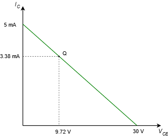
Figure \(\PageIndex{3}\): DC load line for the circuit of Figure \(\PageIndex{2}\).
Note the proportions between voltage and current for the Q point. The voltage is a little less than one-third of the maximum while the current is a little more than two-thirds of its maximum.
5.3.1: Verification of Stability
The claim was made that two-supply emitter bias circuits like the one Figure \(\PageIndex{1}\) potentially have a stable Q point. If we were to plot a second Q point for a large change in \( \beta \), it should hardly move, thus indicating very high stability. For example, doubling \( \beta \) to 200 results in \(I_C = 3.41\) mA and \(V_{CE} = 9.53\) V. The new Q point has edged just slightly closer to saturation, producing about a 1% change in current for a 100% change in \( \beta \). Clearly, this configuration can produce very small changes in the Q point in spite of very large changes in \( \beta \).
5.3.2: Computer Simulation
The two-supply emitter bias circuit of Figure \(\PageIndex{4}\) is simulated using the DC Bias function. A quick estimation shows that we expect about 2 mA of collector current (9.3 V/4.7 k\( \Omega \)) and a collector voltage of about 8 volts (15 V − 2 mA \(\cdot\) 3.6 k\( \Omega \)). We also expect a small negative potential at the base \(−I_BR_B\)). Given typical \( \beta \) values for the 2N3904 (200-ish at this current, refer back to the data sheet), we expect a base current of around 10 to 15 \(\mu\)A, leaving us with a \(V_B\) of approximately −0.1 volts. The emitter voltage would be about 0.7 volts less than that, perhaps −0.8 volts or so.
In short, for a properly designed circuit of this type we expect \(V_B\) to be pretty close to 0 V and \(V_E\) to be about −0.7 volts.
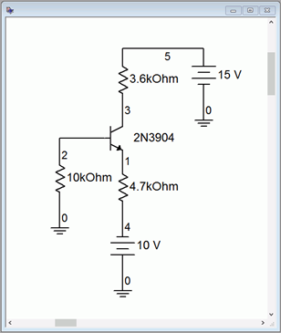
Figure \(\PageIndex{4}\): Schematic for two-supply emitter bias simulation.
The results are shown in Figure \(\PageIndex{5}\). The node voltages agree with our estimations. Node 3 is the collector voltage, very close to the estimation. The results for the base voltage (node 2) and the emitter voltage (node 1) are also in line with the estimates.
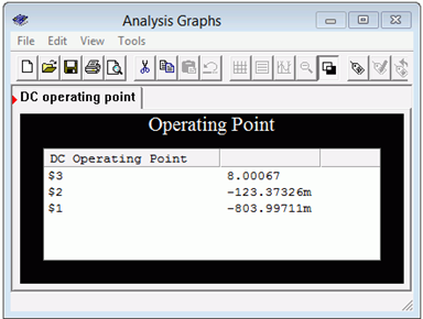
Figure \(\PageIndex{5}\): Simulation results for twosupply emitter bias circuit.
5.3.3: PNP Two-Supply Emitter Bias
While it is possible to create a PNP version of bias circuits by simply swapping out the device and then changing the signs of the power supplies, it is common to “flip” the entire circuit from top to bottom so that the emitter winds up on top and the collector on the bottom. One advantage of this is that, in a multi-transistor circuit schematic, all of the DC bias currents “run down the page”, that is, the collector currents flow from the top of the page to the bottom of the page. Figure \(\PageIndex{6}\) shows a PNP two-supply emitter bias circuit.
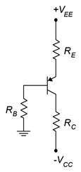
Figure \(\PageIndex{6}\): PNP two-supply emitter bias circuit.
All of the device current equations and component voltage equations derived for the NPN version will hold for the PNP version. The differences to remember are that the voltage polarities will be reversed (what was positive in the NPN is negative in the PNP) and the current directions will be reversed (e.g., conventional current flows into the NPN's collector but out of the PNP's collector. For example, in the NPN we expect the base current to flow into the base terminal. This creates a small negative voltage at the base and a somewhat more negative voltage (by 0.7 V) at the emitter. In the PNP, the base current flows out of the base. This creates a small positive voltage at the base and results in the emitter being slightly more positive (by 0.7 V). This is perhaps best illustrated with an example.
Example \(\PageIndex{2}\)
Assuming \( \beta = 100\), determine the Q point and load line endpoints of the circuit of Figure \(\PageIndex{7}\).
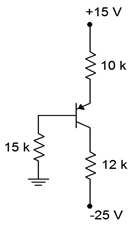
Figure \(\PageIndex{7}\): Circuit for Example \(\PageIndex{2}\).
First, note that this is a PNP drawn upside down so the emitter is at the top. Using Equation \ref{5.1}:
\[I_C = \frac{∣V_{EE}∣−V_{BE}}{R_E+R_B / \beta} \nonumber \]
\[I_C = \frac{15−0.7}{10 k \Omega +15k \Omega /100} \nonumber \]
\[I_C = 1.409mA \nonumber \]
As a cross check, noting the relative sizes of \(R_E\) and \(R_B\), the approximation should be close.
\[I_C = \frac{∣V_{EE}∣−V_{BE}}{R_E} \nonumber \]
\[I_C = \frac{15 −0.7}{10 k \Omega} \nonumber \]
\[I_C = 1.43 mA \nonumber \]
To find \(V_{CE}\) we can use Equation \ref{5.3} with a slight modification.
\[V_{CE} = V_{EE} + ∣V_{CC}∣−I_C (R_C+R_E ) \nonumber \]
\[V_{CE} = 15V+25 V −1.409mA(12 k \Omega +10k \Omega ) \nonumber \]
\[V_{CE} = 9V \nonumber \]
We complete the picture by determining the endpoints of the load line.
\[I_{C(sat)} = \frac{V_{EE} + ∣V_{CC}∣}{R_C+R_E} \nonumber \]
\[I_{C(sat)} = \frac{10 V+25V}{12 K \Omega +10 K \Omega} \nonumber \]
\[I_{C(sat)} = 1.818mA \nonumber \]
\[V_{CE (cutoff )} = V_{EE}+∣V_{CC}∣ \nonumber \]
\[V_{CE (cutoff )} = 15 V+25 V \nonumber \]
\[V_{CE (cutoff )} = 40 V \nonumber \]
The Q point is about 3/4ths of the maximum current and 1/4th of the maximum voltage.