
5.5: Feedback Biasing
- Page ID
- 25415

While two-supply emitter bias and voltage divider bias can produce very high stability, there are other bias configurations available. Their stability tends not to be quite as good, but they are superior to simple base bias. They also tend to use fewer components than their high stability cousins. As a group, we refer to these as feedback biasing configurations. They use the concept of negative feedback. This is a technique where a change in the output can be reflected back to the input in such a way that it tends to partially offset the output change.
5.5.1: Collector Feedback Bias
With a simple move of \(R_B\) in the basic base bias configuration, we arrive at collector feedback bias. The NPN template is shown in Figure \(\PageIndex{1}\). Compared to base bias, all that has changed is that \(R_B\) is connected to the lower part of \(R_C\) rather than to the power supply. That small change can have a noticeable effect on stability.
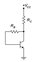
Figure \(\PageIndex{1}\): Collector feedback bias.
To understand how feedback works, assume that a current is flowing from the supply, through \(R_C\), into the collector and finally, out of the emitter to ground. Via KVL, \(V_{CE} = V_C = V_{CC} − I_C \cdot R_C\). Now suppose for some reason, a temperature change perhaps, \(\beta\) increases. This should cause an increase in \(I_C\). An increase in \(I_C\), though, would cause an increase in the drop across \(R_C\) due to Ohm's law. This, in turn, would force \(V_C\) to drop. Here is the key: \(V_C\) is also equal to the drop across \(R_B\) plus the voltage \(V_{BE}\). The base-emitter potential is fixed at approximately 0.7 volts so any decrease in \(V_C\) is reflected as a decrease in voltage across \(R_B\). By Ohm's law, that means that \(I_B\) must decrease by a similar proportion. This decrease tends to offset the initial tendency of the collector current to increase.
To derive an equation for the collector current, we can use KVL.
\[V_{CC} = V_{R_C} +V_{R_B} +V_{BE} \\ V_{CC} = I_E R_C+I_B R_B+V_{BE} \\ V_{CC} = I_C R_C+ \frac{I_C}{\beta} R_B+V_{BE} \\ I_C = \frac{V_{CC} −V_{BE}}{R_C+R_B /\beta} \label{5.10} \]
This equation is very similar to the current derivations for the two-supply emitter bias (Eq 5.3.1) and voltage divider bias (Eq 5.4.3). Again, if we can set \(R_C \gg R_B/\beta\) then \(I_C\) will be relatively immune from Q point shifts due to \(\beta\). The problem here is that it's not nearly so easy to meet that stipulation in this circuit. Consequently, collector feedback tends to have only modest stability.
Concerning the cutoff and saturation endpoints on the DC load line, once again, cutoff is determined by the DC power supply while saturation is determined by the amount of resistance in the collector-emitter to limit said power supply's current.
\[I_{C(sat)} = \frac{V_{CC}}{R_C} \label{5.11} \]
\[V_{CE (cutoff )} = V_{CC} \label{5.12} \]
Example \(\PageIndex{1}\)
Assuming \(\beta = 100\), determine the Q point (\(I_C\) and \(V_{CE}\)) for the circuit of Figure \(\PageIndex{2}\). How much does the Q point change if \(\beta\) is halved?
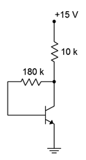
Figure \(\PageIndex{2}\): Circuit for Example \(\PageIndex{1}\).
Using Equation \ref{5.10}
\[I_C = \frac{V_{CC} −V_{BE}}{R_C+R_B /\beta} \nonumber \]
\[I_C = \frac{15 V−0.7 V}{10 k \Omega +180 k \Omega /100} \nonumber \]
\[I_C = 1.21 mA \nonumber \]
Using KVL
\[V_{CE} = V_{CC} −V_{RC} \nonumber \]
\[V_{CE} = V_{CC} −I_C R_C \nonumber \]
\[V_{CE} = 15V−1.21 mA\times 10 k \Omega \nonumber \]
\[V_{CE} = 2.9 V \nonumber \]
If \(\beta\) is halved to 50
\[I_C = \frac{V_{CC} −V_{BE}}{R_C+R_B /\beta} \nonumber \]
\[I_C = \frac{15V−0.7V}{10 k \Omega +180 k \Omega /50} \nonumber \]
\[I_C = 1.05 mA \nonumber \]
\[V_{CE} = V_{CC} −I_C R_C \nonumber \]
\[V_{CE} = 15V−1.05 mA\times 10 k \Omega \nonumber \]
\[V_{CE} = 4.5 V \nonumber \]
For a 2:1 drop in \(\beta\) we see about a 13% reduction in \(I_C\) with a somewhat larger change in \(V_{CE}\). This circuit is clearly not as stable as the two-supply emitter bias or the voltage divider bias but it is superior to base bias.
The PNP version of the collector feedback bias configuration should come as no surprise. The template is shown in Figure \(\PageIndex{3}\). Here, we use the same technique of power supply shifting that was used with the PNP voltage divider in order to wind up with a positive power supply. As with the PNP voltage divider, because we have changed the reference point, all ground referenced voltages will be different from their NPN counterparts. All currents and component voltages will have the same magnitudes but with opposite directions and polarities.
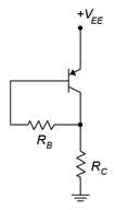
Figure \(\PageIndex{3}\): PNP Collector feedback bias.
5.5.2: Emitter Feedback Bias
The emitter feedback bias uses the same overall idea as the collector feedback circuit, namely, that changes at the output will be reflected back to the input and thus help mitigate the initial change. While collector feedback focuses on collector current establishing \(V_C\) via \(R_C\), emitter feedback uses the fact that emitter current establishes \(V_E\) via \(R_E\). In both cases, these voltages are used to change the voltage across \(R_B\), which results in a change in \(I_B\) that opposes the original collector current change.
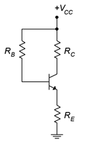
Figure \(\PageIndex{4}\): Emitter feedback bias.
A basic emitter feedback bias circuit is shown in Figure \(\PageIndex{4}\). We shall use KVL to develop an equation for collector current.
\[V_{CC} = V_{R_B} +V_{BE}+V_{R_E} \\ V_{CC} = I_B R_B+V_{BE} + I_E R_E \\ V_{CC} = \frac{I_C}{\beta} R_B + I_C R_E+V_{BE} \\ I_C = \frac{V_{CC} −V_{BE}}{R_E+R_B /\beta} \label{5.13} \]
If we can set \(R_E \gg R_B/\beta\) then the Q point will be stable in spite of changes in \(\beta\). The problem here is the same as was the case in collector feedback, namely that this stipulation is not easy to achieve. Consequently, the emitter feedback configuration tends to have only modest stability. In any event, once the collector current is known, \(V_{CE}\) can be found using the techniques illustrated with the voltage divider configuration. The endpoints for the DC load line are found in the usual manner.
\[I_{C(sat)} = \frac{V_{CC}}{R_C+R_E} \label{5.14} \]
\[V_{CE (cutoff )} = V_{CC} \label{5.15} \]
Example \(\PageIndex{2}\)
Assuming \(\beta\) = 100, determine the Q point (\(I_C\) and \(V_{CE}\)) for the circuit of Figure \(\PageIndex{5}\).
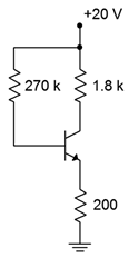
Figure \(\PageIndex{5}\): Circuit for Example \(\PageIndex{2}\).
Using Equation \ref{5.13}
\[I_C = \frac{V_{CC} −V_{BE}}{R_E+R_B /\beta} \nonumber \]
\[I_C = \frac{20 V−0.7V}{200 \Omega +270 k \Omega /100} \nonumber \]
\[I_C = 6.66 mA \nonumber \]
Using KVL
\[V_{CE} = V_{CC} −V_{R_C} −V_{R_E} \nonumber \]
\[V_{CE} = V_{CC} −I_C (R_C+R_E ) \nonumber \]
\[V_{CE} = 20 V−6.66mA(1.8 k \Omega +200 \Omega ) \nonumber \]
\[V_{CE} = 6.68 V \nonumber \]
To complete the load line, we find
\[I_{C(sat)} = 10 mA \nonumber \]
\[V_{CE(cutoff)} = 20 V \nonumber \]
Dropping \(\beta\) to 50 will result in
\[I_C = 3.45 mA \nonumber \]
\[V_{CE} = 13.1 V \nonumber \]
We see less than a 2:1 change in \(I_C\) and \(V_{CE}\) but the stability is not dramatic.
5.5.3: Combination Feedback Bias
The final feedback bias configuration combines both collector feedback and emitter feedback to arrive at the circuit depicted in Figure \(\PageIndex{6}\). We shall bestow upon it the highly original name of combination feedback bias.
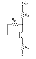
Figure \(\PageIndex{6}\): Combination feedback bias.
This circuit applies feedback to \(R_B\) from both ends, so to speak, so it tends to have slightly better stability than either collector feedback or emitter feedback bias. Of course, it is now only one resistor shy from the voltage divider circuit which is considerably more stable.
The equations for the load line are listed below. The derivations are left as an exercise.
\[I_C = \frac{V_{CC} −V_{BE}}{R_C+R_E+R_B /\beta} \label{5.16} \]
\[V_{CE} = V_{CC} −I_C (R_C+R_E ) \label{5.17} \]
\[I_{C(sat)} = \frac{V_{CC}}{R_C+R_E} \label{5.18} \]
\[V_{CE (cutoff )} = V_{CC} \label{5.19} \]
Example \(\PageIndex{3}\)
Assuming \(\beta = 125\), determine the Q point (\(I_C\) and \(V_{CE}\)) for the circuit of Figure \(\PageIndex{7}\).
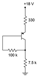
Figure \(\PageIndex{7}\): Circuit for Example \(\PageIndex{3}\).
Note that this is the upside down PNP version. Using Equation \ref{5.16}
\[I_C = \frac{V_{CC} −V_{BE}}{R_C+R_E+R_B /\beta} \nonumber \]
\[I_C = \frac{18 V−0.7V}{7.5 k \Omega +330 \Omega +100 k \Omega / 125} \nonumber \]
\[I_C = 2mA \nonumber \]
Using KVL
\[V_{CE} = V_{CC} −V_{R_C} −V_{R_E} \nonumber \]
\[V_{CE} = V_{CC} −I_C (R_C+R_E ) \nonumber \]
\[V_{CE} = 18V−2 mA(7.5 k \Omega +330 \Omega ) \nonumber \]
\[V_{CE} = 2.34 V \nonumber \]