
5.5: Maximum Power Transfer Theorem
- Page ID
- 25269

The concept of maximum power transfer in DC resistive circuits was presented in earlier work. While maximizing load power is not a goal of all circuit designs, it is a goal of a portion of them and thus worth a closer look. In short, given an AC voltage source with internal impedance, as seen in Figure \(\PageIndex{1}\), a useful question to ask is “What value of load impedance will yield the maximum amount of power in the load?” In the DC case, it was discovered that the load resistance must equal the source resistance in order to achieve maximum load power. In the AC case things appear to be much more complicated by the possible presence of reactances in both the source and load.
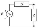
As a refresher of prior study, consider the basic circuit depicted in Figure \(\PageIndex{1}\) with source \(E\), source internal resistance \(Z_i\) and load impedance \(Z\). For the moment, we shall ignore the reactive portions and just describe the load power in terms of the load's resistive portion, \(R\). To make the job easier, we may normalize the source resistance \(R_i\) to 1 \(\Omega\). By doing this, \(R\) also becomes a normalized value, that is, it no longer represents a simple resistance value but rather represents a ratio in comparison to \(R_i\). In this way the analysis will work for any set of source values. Note that the value of \(E\) will equally scale the power in both \(R_i\) and \(R\), so a precise value is not needed, and thus, we may as well chose 1 volt for convenience.
The power in the load can be determined by using \(I^2 R\) where \(I = E / (R_i+R)\), yielding
\[P = \left( \frac{E}{R_i+R} \right)^2 R \nonumber \]
Using our normalized values of 1 volt and 1 \(\Omega\),
\[P = \left( \frac{1}{1+R} \right)^2 R \nonumber \]
After expanding we arrive at:
\[P = \frac{R}{R^2 + 2 R+1} \label{5.1} \]
We now have an equation that describes the load power in terms of the load resistance. Before we go any further, take a look at what this equation tells you, in general. It is obvious that maximum power will not occur at the extremes. If \(R = 0\) or \(R = \infty \) (i.e., shorted or opened load) the load power is zero. The maximizing case occurs somewhere in the middle. To find the precise value that produces the maximum load power, the proof can be divided into two portions. The first involves graphing the function and the second requires differential calculus to solve for a precise value. We shall proceed with the graphing portion which will lead us to the answer. The more rigorous proof of the second portion is detailed in Appendix C.
The curve of Equation \ref{5.1} is plotted in Figure \(\PageIndex{2}\). The normalized load resistance is set along the horizontal and the normalized power (i.e., for a source of 1 volt) is set along the vertical.
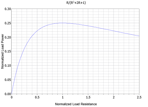
An examination of the power curve shows that the peak occurs at \(R = 1\). In other words, the load must be equal to the source resistance. Thus, we can say that if no reactances are involved, maximum load power occurs when the load resistance equals the source resistance. It does not matter if the source is DC or AC.
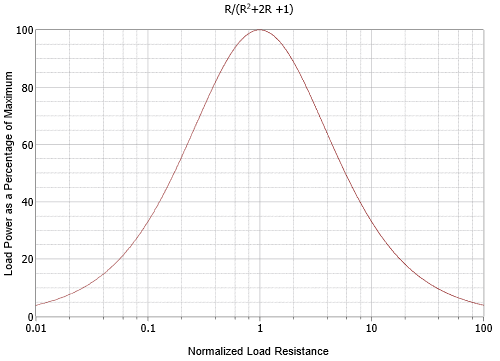
The graph shown in Figure \(\PageIndex{2}\) is asymmetric but the concept of resistance ratios is key here. This is easier to see if we plot the completed power curve using a logarithmic horizontal axis and also scale the vertical axis to 100%, as shown in Figure \(\PageIndex{3}\). The peak is more apparent and the curve is symmetrical in shape rather than lopsided. This reinforces the idea that the ratio of the resistances is what matters.
At this point we may turn our attention to the possible presence of reactances in both the source and load. It turns out that this is not nearly as complicated as it might look. The key is that only resistors dissipate power, not inductors or capacitors1. Load power is proportional to \(i_{load}^2\), so our immediate goal is to maximize load current for any set of source and load resistances.
We can modify the original power equation by adding a new term, \(X\), which represents the net reactance in the circuit. In other words, \(X\) is equal to the sum of the reactances in the source impedance and load impedance. The power in the load is still determined by using \(I^2 R\), however, we must now include the \(X\) term when computing the current:
\[I = \frac{E}{\sqrt{((R_i+R)^2+X^2 )} \nonumber \]
This leads is to a new load power expression:
\[P = \left( \frac{E}{\sqrt{((R_i+R)^2+X^2 ) \right)^2 R \label{5.2} \]
A cursory look at Equation \ref{5.2} shows that to maximize \(P\), \(X\) must be zero. A normalized plot of this equation is shown in Figure \(\PageIndex{4}\) for \(R = R_i\).
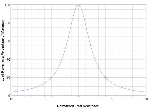
A single peak is evident when \(X\) is 0. This can be achieved by setting the load reactance equal in magnitude to the source reactance but with the opposite sign. In this manner, the reactances will cancel out, leaving a purely resistive circuit with a minimal value, and thus producing maximal current for that set of resistors.
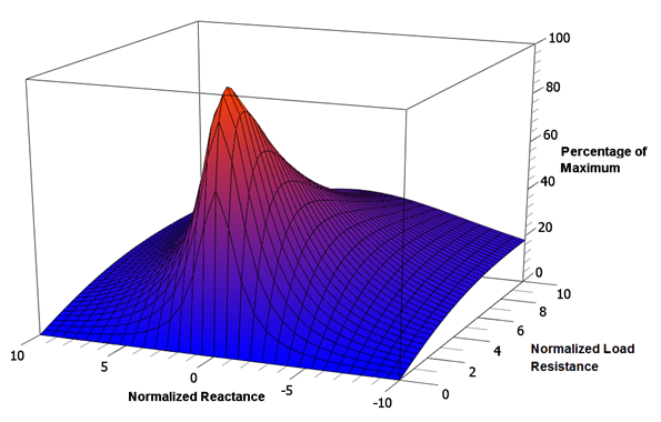
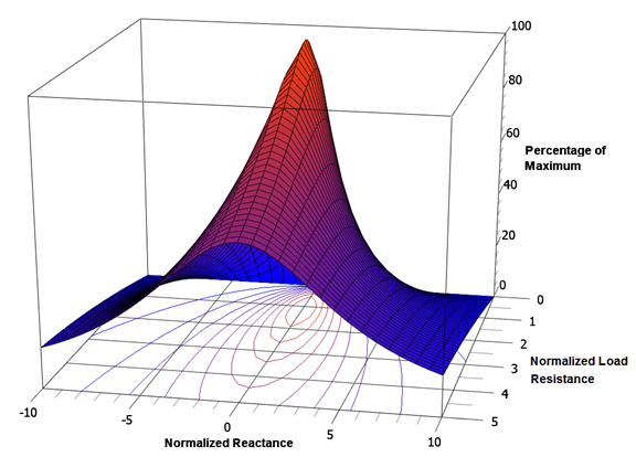
Two variables are involved here, so to further clarify the situation, a 3D surface plot of normalized power is shown in Figure \(\PageIndex{5}\). The vertical axis represents the percentage of maximum power while the front and side axes are the normalized total reactance and load resistance, respectively. A single peak is evident here and coincides with \(X = 0\) and \(R = 1\). This is more easily seen by viewing the surface from the back as shown in Figure \(\PageIndex{6}\). Note that the highest isocontour encircles the intersection of \(X = 0\) and \(R = 1\) (i.e., \R_{load} = R_i\)).
In sum, we have verified that the resistive portions of the source and load impedance must be identical and that the reactive portions must be of the same magnitude but of opposite sign. This configuration is also known as the complex conjugate. Finally, we can state:
\[\text{Maximum load power will be achieved when the load impedance is equal to the complex conjugate of the internal impedance of the driving source.} \nonumber \]
No other value of load impedance will produce a higher load power. We can imagine two general cases, one with an inductive source impedance and another with a capacitive source impedance. These are shown with the proper loads in Figure \(\PageIndex{7}\).
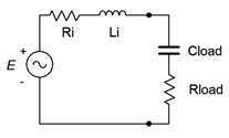
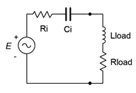
To achieve maximum load power in these circuits, \(R_{load} = R_i\) and \(|jX_L| = |−jX_C|\). Note that \(X_L\) and \(X_C\) do not have to have the same magnitude as \(R_i\).
While using the complex conjugate produces the maximum load power, it does not produce the largest possible load current or load voltage. In fact, this condition produces a load voltage and a load current that are half of their maximums. Their product, however, is at the maximum. Further, efficiency at maximum load power is only 50% (i.e., only half of all generated power goes to the load with the other half being wasted internally). Values of \(R\) greater than \(R_i\) will achieve higher efficiency but at reduced load power. Sometimes we favor efficiency over maximal load power.
As any linear single port network can be reduced to something like Figure \(\PageIndex{7}\) by using Thévenin's theorem, combining the two theorems allows us to determine maximum power conditions for any impedance in a complex circuit.
Example \(\PageIndex{1}\)
Consider the circuit of Figure \(\PageIndex{8}\). What is the power generated in the load if it is equal to 40 \(\Omega\)? Further, is that the maximum power that can be attained, and if not, what is the maximum load power and what value of load would be needed?
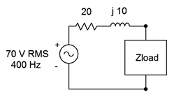
To find the load power, first find the circulating current, then use power law. The total impedance seen by the source is \(20 + j10 \Omega + 40 \Omega\), or \(60 + j10 \Omega\).
\[i = \frac{E}{Z_{total}} \nonumber \]
\[i = \frac{70V}{60\Omega +j 10\Omega} \nonumber \]
\[i = 1.151\angle −9.5^{\circ} A \nonumber \]
As the voltage and current are in phase for a resistor, we can ignore the angle for the power calculation.
\[P_{load} = i^2 \times R_{load} \nonumber \]
\[P_{load} = (1.151A)^2 \times 40\Omega \nonumber \]
\[P_{load} \approx 53W \nonumber \]
This is not the maximum load power that can be achieved because this load is not the complex conjugate of the source impedance. The required load for maximum load power is shown in Figure \(\PageIndex{9}\).
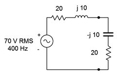
We shall repeat the process to find the new load power.
\[i = \frac{E}{Z_{total}} \nonumber \]
\[i = \frac{70 V}{40\Omega} \nonumber \]
\[i = 1.75 \angle 0^{\circ} A \nonumber \]
\[P_{load} = i^2 \times R_{load} \nonumber \]
\[P_{load} = (1.75 A)^2 \times 20 \Omega \nonumber \]
\[P_{load} = 61.25W \nonumber \]
An alternate method notes that the new circuit's total impedance is purely resistive and that the source and load resistances are identical. Therefore the voltage source must split evenly across them. In this case that's 35 volts RMS each.
\[P_{load} = \frac{v_R^2}{R_{load}} \nonumber \]
\[P_{load} = \frac{(35 V)^2}{20\Omega} \nonumber \]
\[P_{load} = 61.25W \nonumber \]
Example \(\PageIndex{2}\)
For the circuit of Figure \(\PageIndex{10}\), determine the value of \(Z_{load}\) that will achieve maximum load power and also determine that power. The current source is \(0.1\angle 0^{\circ}\) amps RMS at 50 kHz.
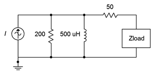
The first job is determine the inductive reactance at 50 kHz. Recalling that \(X_L = j2\pi fL\), this works out to \(j157 \Omega\). We now need to find the Thévenin equivalent. To find \(Z_{th}\) we open the current source and look back in from the load. We see the 50 \(\Omega\) resistor in series with the parallel combination of the 200 \(\Omega\) resistor and the inductor. The parallel combination is:
\[Z = \frac{R \times jX_L}{R +jX_L} \nonumber \]
\[Z = \frac{200 \Omega \times ( j 157 \Omega )}{200\Omega +j 157\Omega} \nonumber \]
\[Z = 76.3+j 97.2\Omega \nonumber \]
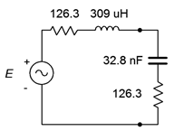
Therefore, \(Z_{th} = 126.3 + j97.2 \Omega\). The complex conjugate is \(126.3 − j97.2 \Omega\). The capacitive reactance formula may be used to determine the appropriate capacitance value to achieve \(−j97.2 \Omega\).
\[C = \frac{1}{2 \pi f X_C} \nonumber \]
\[C = \frac{1}{2\pi 50 kHz 97.2\Omega} \nonumber \]
\[C = 32.8 nF \nonumber \]
The resulting circuit is shown in Figure \(\PageIndex{11}\).
To find the load power we need to find \(E_{th}\). The open circuit output voltage is the potential appearing across the inductor/resistor pair in Figure \(\PageIndex{10}\). This is because there is no current flowing through the 50 \(\Omega\) resistor, and therefore there is no voltage across it. \(E_{th}\) can be found via Ohm's law as we already know the impedance of the parallel branch.
\[E_{th} = i\times Z \nonumber \]
\[E_{th} = 0.1\angle 0^{\circ} A\times (76.3+j 97.2\Omega ) \nonumber \]
\[E_{th} = 12.4\angle 51.9^{\circ} V \nonumber \]
Again, using the complex conjugate, the voltage source splits evenly between the resistive components. As the current source was specified as RMS, so too will be the equivalent voltage.
\[P_{load} = \frac{v_R^2}{R_{load}} \nonumber \]
\[P_{load} = \frac{(6.2 V)^2}{126.3\Omega} \nonumber \]
\[P_{load} = 304.4mW \nonumber \]
This represents the maximum load power that can be achieved in this circuit. Do not forgot, though, that an equal amount of power is dissipated by the source. This produces an efficiency of just 50%.
In summation, we can say that maximum load power is achieved when the load impedance is equal to the complex conjugate of the internal impedance of the circuitry driving the load. Usually, this requires the application of either a Thévenin or Norton equivalent. Finally, although maximum power transfer is a desired outcome in some situations, it is not desirable in all situations. The reason is one of efficiency. At the maximum load power, efficiency is only 50%. In contrast, for load impedances that are greater than the source impedance, the load power will decrease, however, the efficiency will increase. Increased efficiency is particularly important when striving to minimize heat and extend battery life.
References
1Power in AC circuits is examined in great detail in Chapter 7.