
8.6: Implementing the 74153 Circuit
- Page ID
- 27000

\( \newcommand{\vecs}[1]{\overset { \scriptstyle \rightharpoonup} {\mathbf{#1}} } \) \( \newcommand{\vecd}[1]{\overset{-\!-\!\rightharpoonup}{\vphantom{a}\smash {#1}}} \)\(\newcommand{\id}{\mathrm{id}}\) \( \newcommand{\Span}{\mathrm{span}}\) \( \newcommand{\kernel}{\mathrm{null}\,}\) \( \newcommand{\range}{\mathrm{range}\,}\) \( \newcommand{\RealPart}{\mathrm{Re}}\) \( \newcommand{\ImaginaryPart}{\mathrm{Im}}\) \( \newcommand{\Argument}{\mathrm{Arg}}\) \( \newcommand{\norm}[1]{\| #1 \|}\) \( \newcommand{\inner}[2]{\langle #1, #2 \rangle}\) \( \newcommand{\Span}{\mathrm{span}}\) \(\newcommand{\id}{\mathrm{id}}\) \( \newcommand{\Span}{\mathrm{span}}\) \( \newcommand{\kernel}{\mathrm{null}\,}\) \( \newcommand{\range}{\mathrm{range}\,}\) \( \newcommand{\RealPart}{\mathrm{Re}}\) \( \newcommand{\ImaginaryPart}{\mathrm{Im}}\) \( \newcommand{\Argument}{\mathrm{Arg}}\) \( \newcommand{\norm}[1]{\| #1 \|}\) \( \newcommand{\inner}[2]{\langle #1, #2 \rangle}\) \( \newcommand{\Span}{\mathrm{span}}\)\(\newcommand{\AA}{\unicode[.8,0]{x212B}}\)
Figure \(\PageIndex{2}\) shows the final implementation of the 74153 input mirroring circuit, as well as indicating the steps to be followed in implementing the circuit. These steps correspond to the numbers in the following list.
- Install 2 switches and 2 LEDs.
- Install and power the 74153 chip. Figure \(\PageIndex{1}\) is the 74153 pin configuration diagram. Most of the pins will be hardwired to values, which will be explained in the following list. Pins which are wired to other components in the circuit are explained in subsequent steps.
Figure \(\PageIndex{1}\): 74153 pin configuration diagram 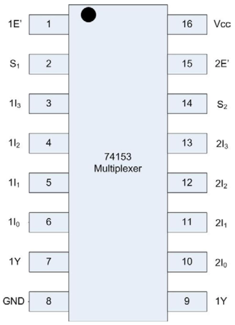
- Pins 1 (1E') and 15 (2E') are enable low pins. Enable both multiplexers by connecting these pins to ground.
- Pins 3..6 and 10..14 are the input values to the MUX. These are to be programmed as in Figure \(\PageIndex{1}\). Pins 3..6 are values 0011, and pins 10..14 are 0101. 0 values are connected to the ground rail, 1 values are connected to the positive rail.
- Connect the switches to the input select values for the MUXes. Connect Switch 1 to S1 (pin 2), and Switch 2 to S2 (pin 15).
- Connect the output Y values to the LEDs.
Figure \(\PageIndex{2}\): 74153 circuit 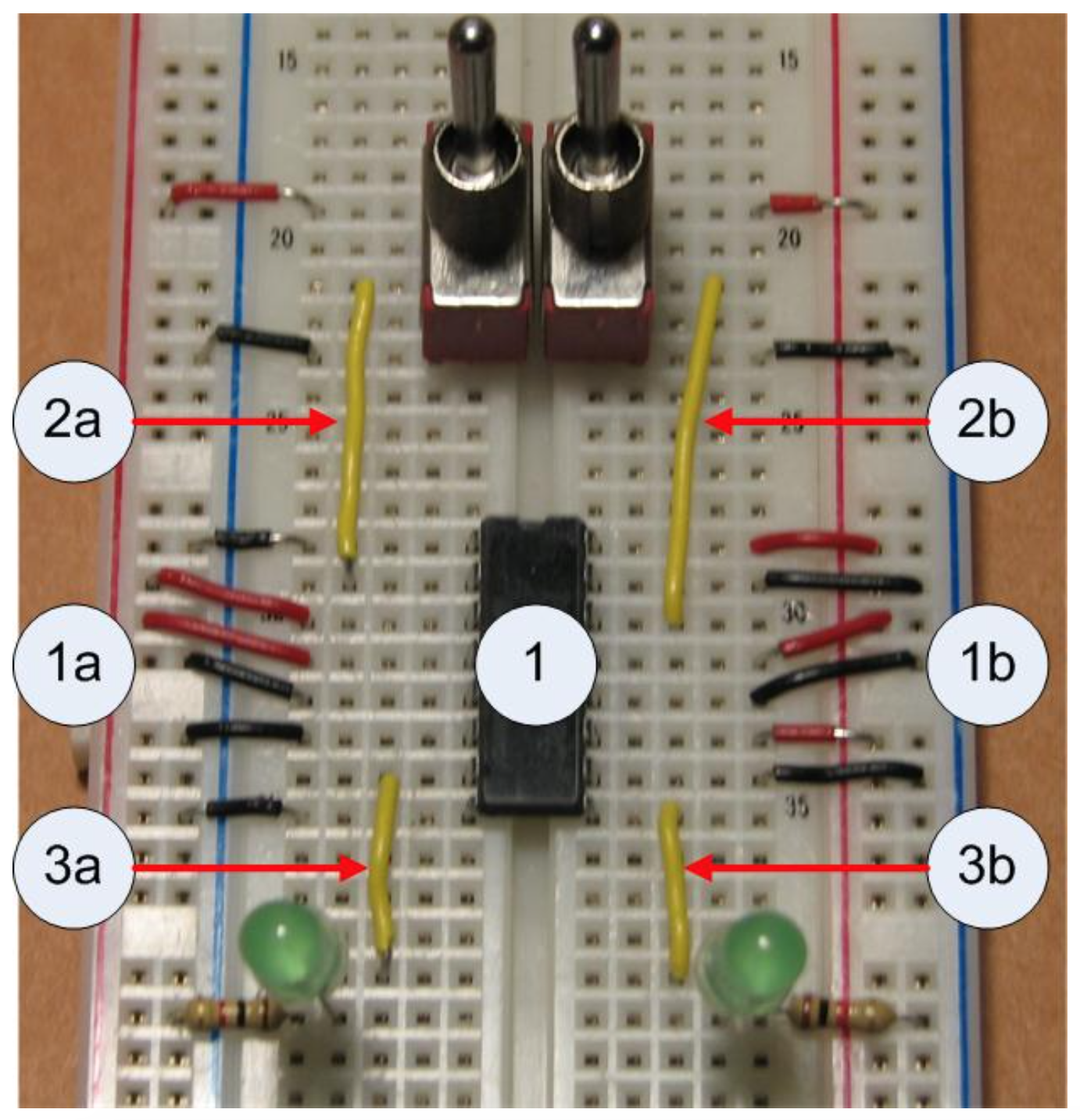
The circuit should now mirror the input switches.