
11.1: An Overview of the CPU
- Page ID
- 26883

The following figure is of the entire CPU that will be covered in this text. There are 3 Logisim sub circuits that are part of this CPU, two of which will be broken down to show how the ICs from this book. They are the Arithmetic Logic Unit (ALU), and the Control Unit (CU). These two units will be explained in terms of the entire CPU, and then shown as sub circuits to expose the decoder and adder circuits.
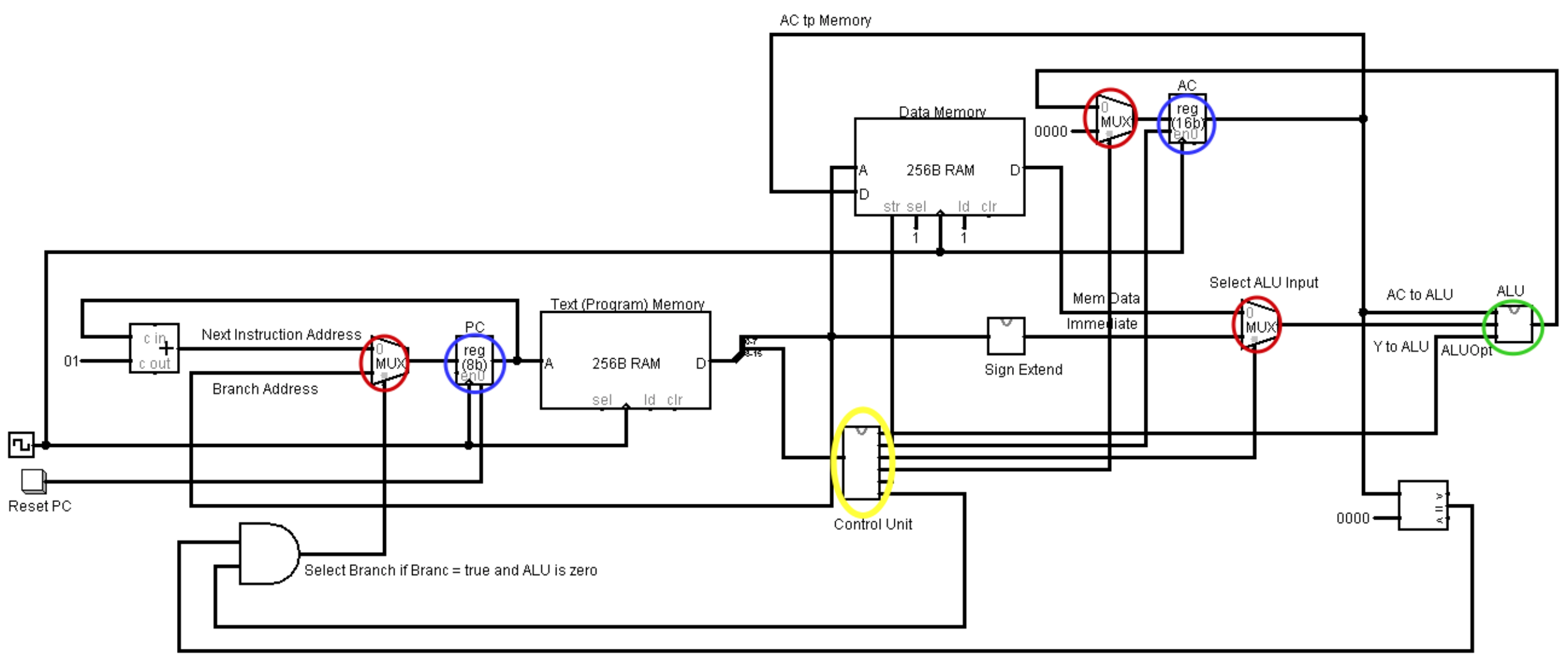
This CPU is an example of an accumulator or one-address architecture CPU. In all CPU designs, two operands are feed to the ALU, where the two operands are used to perform some operation and produce a result. In an Accumulator CPU, one of these operands is called the $pc, which is memory on the CPU chip (called a register), and the other comes from either the instruction itself or memory. So a simple program to add two numbers, the value of variable A and the number 2, would look as follows:
| clac |
# set the $ac (accumulator register) to 0 |
| add A |
# add the value of A to the accumulator |
| addi 5 |
# add the number 5 to the value in the accumulator |
| stor B |
# stor the accumulator value to memory variable B |
The CPU keeps track of the statement to process using the Program Counter ($pc) register. The $pc contains the address of the next instruction to execute. The CU takes the instruction, which is a 4-bit binary number, and breaks it down into control wires which specify how each component of the CPU (muxes, decoders, ALU, and memory) should behave for that instruction. The ALU does the actual operation that is requested (e.g. an add, subtract, etc.)
So for example the add A instruction. The CU would specify:
- That the mux in front of the $pc select the input 0, which is the next instruction in the program (e.g. do not branch).
- That the mux in front of the $ac select input 0, which is the result of the ALU, to store in the $ac.
- That the mux in front of the ALU select a value from memory, not the instruction.
- That the ALU execution an addition operation.
- That the value of the $ac not be stored back to memory.
The rest of this chapter will show how the IC’s from this text are used in this design.