
4.1: Introduction
- Page ID
- 41275

The majority of transmission lines used in high-speed digital, RF, and microwave circuits are planar, as these can be defined using masks, photoresist, and etching of metal sheets. Such lines are called planar transmission lines. A common planar line is the microstrip line shown in Figure \(\PageIndex{1}\) and in cross section in Figure \(\PageIndex{2}\). This cross section is typical of what would be found on a semiconductor or printed circuit board (PCB). Current flows in both the top and bottom conductor, but in opposite directions. The physics is such that if there is a signal current on the top
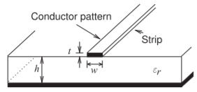
Figure \(\PageIndex{1}\): Microstrip transmission line.
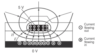
Figure \(\PageIndex{2}\): Cross-sectional view of a microstrip line showing electric and magnetic field lines and current flow. The electric and magnetic fields are in two mediums—the dielectric and air. If the line is homogeneous (the same dielectric everywhere) the electric and magnetic fields are only in the transverse plane, a field configuration known as the transverse electromagnetic mode (TEM).
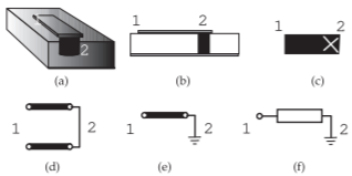
Figure \(\PageIndex{3}\): Representations of a shorted microstrip line with a short (or via) at port 2: (a) threedimensional (3D) view indicating via; (b) side view; (c) top view with via indicated by \(\mathsf{X}\); (d) schematic representation of transmission line; (e) alternative schematic representation; and (f) representation as a circuit element.
conductor, there must be a return signal current, which will be as close to the signal current as possible to minimize stored energy. The provision of a signal return path is important in maintaining the integrity of (i.e., a predictable signal waveform on) an interconnect.
predictable signal waveform on) an interconnect. In the microstrip line, electric field lines start on one of the conductors and finish on the other and are located almost entirely in the plane transverse to the long length of the line. The magnetic field is also mostly confined to the transverse plane, and so this line is referred to as a transverse electromagnetic (TEM) line. More accurately it is called a quasi-TEM line, as the longitudinal fields, particularly in the air region, are not negligible.
Various schematic representations of a microstrip line are used. Consider the representations in Figure \(\PageIndex{3}\) of a length of microstrip line shorted by a via at the end denoted by “\(2\)” (specifically the “\(2\)” refers to Port 2).