
6.2: Physics of Coupling
- Page ID
- 41291

If the fields of one transmission line intersect the region around another transmission line, then some of the energy propagating on the first line appears on the second. This coupling discriminates in terms of forward- and backward-traveling waves. In particular, consider the coupled microstrips shown in Figure \(\PageIndex{1}\). The direction of propagation comes from \(\overline{\mathcal{E}}\times\overline{\mathcal{H}}\). Using the right-hand rule, the direction of propagation of the signal on the lefthand strip is out of the page. This is called the forward-traveling direction. Now consider the fields around the right-hand strip, the inactive line, and note the direction of the \(E\) field. The \(H\) field immediately to the left of the
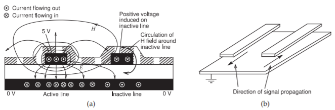
Figure \(\PageIndex{1}\): Edge-coupled microstrip lines with the left line driven with the forward-traveling field coming out of the page: (a) cross section of microstrip lines as found on a printed circuit board showing a conformal top passivation or solder resist layer; and (b) in perspective showing the direction of propagation of the driven line (left) and the direction of propagation of the main coupled signal on the victim line (right).
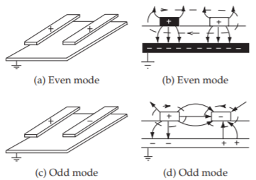
Figure \(\PageIndex{2}\): Modes on parallel-coupled microstrip lines. In (b) and (d) the electric fields are indicated as arrowed lines and the magnetic field lines are dashed.
right-hand strip is stronger than on the right of the strip. So effectively there is a clockwise circulation of the \(\mathcal{H}\) field around the right hand strip. By applying \(\overline{\mathcal{H}}\times\overline{\mathcal{H}}\) to the signal induced on the right-hand strip, it is seen that the induced signal travels into the page, or in the backward-traveling direction. The coupling with parallel-coupled microstrip lines is called backward-wave coupling. Both the even mode and the odd mode, and both have forwardand backward-traveling components (see Figure \(\PageIndex{2}\)).
In the even mode (Figures \(\PageIndex{2}\)(a and b)), the amplitude and polarity of the voltages on the two signal conductors are the same. In the odd mode (Figures \(\PageIndex{2}\)(c and d)), the voltages on the two signal conductors are equal but have opposite polarity. Any EM field orientation on the coupled lines can be represented as a weighted addition of the even-mode and odd-mode field configurations. The actual fields will be a superposition of the even and odd modes. Also the voltages on the lines are composed of even and odd components.
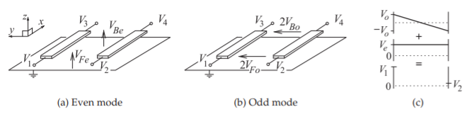
Figure \(\PageIndex{3}\): Definitions of total voltages and even- and odd-mode voltage phasors on a pair of coupled microstrip lines: (a) even-mode voltage definition; (b) odd-mode voltage definition; (c) depiction of how even- and odd-mode voltages combine to yield the total voltages on individual lines. \(F\) indicates front and \(B\) indicates back.
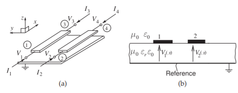
Figure \(\PageIndex{4}\): Coupled microstrip lines: (a) with total voltage and current phasors at the four terminals; and (b) cross section.
The characteristic impedances of the even and odd modes will differ because of the different field orientations. These are termed the evenmode and odd-mode characteristic impedances, denoted by \(Z_{0e}\) and \(Z_{0o}\), respectively. Here the \(e\) subscript identifies the even mode and the \(o\) subscript identifies the odd mode. With coupled microstrip lines, the phase velocities of the two modes will differ since the two modes have different amounts of energy in the air and in the dielectric, resulting in different effective permittivities of the two modes.
Coupled lines are modeled by determining the propagation characteristics of the even and odd modes. Using the definitions shown in Figures \(\PageIndex{3}\) and \(\PageIndex{4}\), the total voltage and current phasors on the original structure are a superposition of the even- and odd-mode solutions:
\[\label{eq:1}\left.\begin{array}{ll}{V_{1}=V_{Fe}+V_{Fo}}&{I_{1}=I_{Fe}+I_{Fo}}\\{V_{2}=V_{Fe}-V_{Fo}}&{I_{2}=I_{Fe}-I_{Fo}}\\{V_{3}=V_{Be}+V_{Bo}}&{I_{3}=I_{Be}+I_{Bo}}\\{V_{4}=V_{Be}-V_{Bo}}&{I_{4}=I_{Be}-I_{Bo}}\end{array}\right\} \]
with the subscripts \(F\) and \(B\) indicating the front and back, respectively, of the even- and odd-mode components. Also
\[\label{eq:2}\left.\begin{array}{ll}{V_{Fe}=(V_{1}+V_{2})/2}&{I_{Fe}=(I_{1}+I_{2})/2}\\{V_{Fo}=(V_{1}-V_{2})/2}&{I_{Fo}=(I_{1}-I_{2})/2}\\{V_{Be}=(V_{3}+V_{4})/2}&{I_{Be}=(I_{3}+I_{4})/2}\\{V_{Bo}=(V_{3}-V_{4})/2}&{I_{Bo}=(I_{3}-I_{4})/2}\end{array}\right\} \]
The forward-traveling components can be written as
\[\label{eq:3}\left.\begin{array}{ll}{V_{1}^{+}=V_{Fe}^{+}+V_{Fo}^{+}}&{I_{1}^{+}=I_{Fe}^{+}+I_{Fo}^{-}}\\{V_{2}^{+}=V_{Fe}^{+}-V_{Fo}^{+}}&{I_{2}^{+}=I_{Fe}^{+}-I_{Fo}^{-}}\\{V_{3}^{+}=V_{Be}^{+}+V_{Bo}^{+}}&{I_{3}^{+}=I_{Be}^{+}+I_{Bo}^{-}}\\{V_{4}^{+}=V_{Be}^{+}-V_{Bo}^{+}}&{I_{4}^{+}=I_{Be}^{+}-I_{Bo}^{-}}\end{array}\right\} \]
The backward-traveling components are written similarly so that the total front and back even- and odd-mode voltages are
\[\label{eq:4}\left.\begin{array}{ll}{V_{Fe}=V_{Fe}^{+}+V_{Fe}^{-}}&{V_{Be}=V_{Be}^{+}+V_{Be}^{-}}\\{V_{Fo}=V_{Fo}^{+}+V_{Fo}^{-}}&{V_{Bo}=V_{Bo}^{+}+V_{Bo}^{-}}\end{array}\right\} \]
With an ideal voltmeter the \(V_{1},\: V_{2},\: V_{3},\) and \(V_{4}\) voltages would be measured from a point on the strip to a point on the ground plane immediately below. The voltages \(2V_{Fo}\) and \(2V_{Bo}\) are the voltages that would be measured between the strips at the front and back of the lines, respectively (see Figure \(\PageIndex{2}\)). It would not be possible to directly measure \(V_{Fe}\) and \(V_{Be}\).
One set of network parameters describing a pair of coupled lines is the port-based admittance matrix equation relating the port voltages, \(V_{1}–V_{4}\), to the port currents, \(I_{1}–I_{4}\):
\[\label{eq:5}\left[\begin{array}{l}{I_{1}}\\{I_{2}}\\{I_{3}}\\{I_{4}}\end{array}\right] =\left[\begin{array}{llll}{y_{11}}&{y_{12}}&{y_{13}}&{y_{14}}\\{y_{21}}&{y_{22}}&{y_{23}}&{y_{24}}\\{y_{31}}&{y_{32}}&{y_{33}}&{y_{34}}\\{y_{41}}&{y_{42}}&{y_{43}}&{y_{44}}\end{array}\right] \left[\begin{array}{l}{V_{1}}\\{V_{2}}\\{V_{3}}\\{V_{4}}\end{array}\right] \]
These are port-based \(y\) parameters as the currents and voltages are defined for ports. Since microstrip lines are fabricated (most of the time) on nonmagnetic dielectrics, then they are reciprocal so that \(y_{ij} = y_{ji}\). Coupling from one line to another is described by the terms \(y_{12} (=y_{21})\) and \(y_{34} (=y_{43})\).
6.2.1 Summary
The important concept introduced in this section is that fields and the propagating waves on a pair of parallel coupled lines can be described as a combination of odd and even modes each of which has forward- and backward-wave versions.