
10.3: Impedance Transforming Networks
- Page ID
- 41325

Transformers and reactive elements considered in this section can be used to losslessly transform impedance levels. his is a basic aspect of network design.
10.3.1 The Ideal Transformer
The ideal transformer shown in Figure 10.2.2 can be used to match a load to a source if the source and load impedances are resistances. This will be shown by starting with the constitutive relations of the transformer:
\[\label{eq:1}V_{1}=nV_{2}\quad\text{and}\quad I_{1}=-I_{2}/n \]
Here \(n\) is the transformer ratio. For a wire-wound transformer, \(n\) is the ratio of the number of windings on the primary side, Port \(1\), to the number of windings on the secondary side, Port \(2\). Thus the input resistance, \(R_{\text{in}}\), is related to the load resistance, \(R_{L}\), by
\[\label{eq:2}R_{\text{in}}=\frac{V_{1}}{I_{1}}=-n^{2}\frac{V_{2}}{I_{2}}=n^{2}R_{L} \]
The matching problem with purely resistive load and source impedances is solved by choosing the appropriate winding ratio, \(n\). However, resistive-only problems are rare at RF, and so other matching circuits must be used.
10.3.2 A Series Reactive Element
Matching using lumped elements is based on the impedance and admittance transforming properties of series and shunt reactive elements. Even a single reactive element can achieve limited impedance matching. Consider the series reactive element shown in Figure 10.2.3(a). Here the reactive element, \(X_{S}\), is in series with a resistance \(R\). The shunt equivalent of this network is shown in Figure 10.2.3(b) with a shunt susceptance of \(B\). In this transformation the resistance \(R\) has been converted to a resistance \(R_{P}= 1/G\). The mathematics describing this transformation is as follows. The input admittance of the series connection (Figure 10.2.3(a)) is
\[\label{eq:3}Y_{\text{in}}(\omega )=\frac{1}{Z_{\text{in}}(\omega )}=\frac{1}{R+\jmath X_{S}}=\frac{R}{R^{2}+X_{S}^{2}}-\jmath\frac{X_{S}}{R^{2}+X_{S}^{2}} \]
Thus the elements of the equivalent shunt network, Figure 10.2.3(b), are
\[\label{eq:4}G=\frac{R}{R^{2}+X_{S}^{2}}\quad\text{and}\quad B=-\frac{X_{S}}{R^{2}+X_{S}^{2}} \]
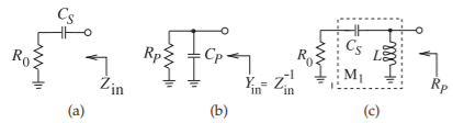
Figure \(\PageIndex{1}\): Impedance transformation by a series reactive element: (a) a resistor with a series capacitor; (b) its equivalent shunt circuit; and (c) an \(LC\) network.
The “resistance” of the network, \(R\), has been transformed to a new value,
\[\label{eq:5}R_{P}=G^{-1}=\frac{R^{2}+X_{S}^{2}}{R}>R \]
This is an important start to matching, as \(X_{S}\) can be chosen to convert \(R\) (a load, for example) to any desired resistance value (such as the resistance of a source). However there is still a residual reactance that must be removed to complete the matching network design. Before moving on to the solution of this problem consider the following example.
Example \(\PageIndex{1}\): Capacitive Impedance Transformation
Consider the impedance transforming properties of the capacitive series element in Figure \(\PageIndex{1}\)(a). Show that the capacitor can be adjusted to obtain any positive shunt resistance.
Solution
The concept here is that the series resistor and capacitor network has an equivalent shunt circuit that includes a capacitor and a resistor. By adjusting \(C_{S}\) any value can be obtained for \(R_{P}\). From Equation \(\eqref{eq:5}\),
\[\label{eq:6}R_{P}=\frac{R_{0}^{2}+(1/\omega^{2}C_{S}^{2})}{R_{0}}=\frac{1+\omega ^{2}C_{S}^{2}R_{0}^{2}}{\omega ^{2}C_{S}^{2}R_{0}} \]
and the susceptance is
\[\label{eq:7}B=\frac{(1/\omega C_{S})}{R_{0}^{2}+1/\omega ^{2}C_{S}^{2}}=\omega\frac{C_{S}}{1+\omega ^{2}C_{S}^{2}R_{0}^{2}} \]
Thus
\[\label{eq:8}C_{P}=\frac{B}{\omega}=\frac{C_{S}}{1+\omega ^{2}C_{S}^{2}R_{0}^{2}} \]
To match \(R_{0}\) to a resistive load \(R_{P}\) (\(> R_{0}\)) at a radian frequency \(\omega_{d}\), then, from Equation \(\eqref{eq:6}\), the series capacitance required, i.e. the design equation for \(C_{S}\), comes from
\[\label{eq:9}\omega _{d}C_{S}=1/\sqrt{R_{0}R_{P}-R_{0}^{2}} \]
To complete the matching design, use a shunt inductor \(L\), as shown in Figure \(\PageIndex{1}\)(c), where \(\omega_{d}C_{P} = 1/(\omega_{d}L)\). The equivalent impedance in Figure \(\PageIndex{1}\)(c) is a resistor of value \(R_{P}\), with a value that can be adjusted by choosing \(C_{S}\) which then requires \(L\) to be adjusted.
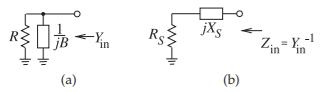
Figure \(\PageIndex{2}\): A resistor with (a) a shunt parallel reactive element where \(B\) is a susceptance, and (b) its equivalent series circuit.
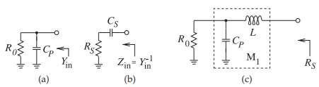
Figure \(\PageIndex{3}\): Parallel-to-series transformation: (a) resistor with shunt capacitor; (b) its equivalent series circuit; and (c) the transforming circuit with added series inductor.
10.3.3 A Parallel Reactive Element
The dual of the series matching procedure is the use of a parallel reactive element, as shown in Figure \(\PageIndex{2}\)(a). The input admittance of the shunt circuit
\[\label{eq:10}Y_{\text{in}}=\frac{1}{R}+\jmath B \]
This can be converted to a series circuit by calculating \(Z_{\text{in}} = 1/Y_{\text{in}}\):
\[\label{eq:11}Z_{\text{in}}=\frac{R}{1+\jmath BR}=\frac{R}{1+B^{2}R^{2}}-\jmath\frac{BR^{2}}{1+B^{2}R^{2}} \]
So
\[\label{eq:12}R_{S}=\frac{R}{1+B^{2}R^{2}}\quad\text{and}\quad X_{S}=\frac{-BR^{2}}{1+B^{2}R^{2}} \]
Notice that \(R_{S} < R\).
Example \(\PageIndex{2}\): Parallel Tuning
As an example of the use of a parallel reactive element to tune a resistance value, consider the circuit in Figure \(\PageIndex{3}\)(a) where a capacitor tunes the effective resistance value so that the series equivalent circuit (Figure \(\PageIndex{3}\)(b)) has elements
\[\label{eq:13}R_{S}=\frac{R_{0}}{1+\omega ^{2}C_{P}^{2}R_{0}^{2}}\quad\text{and}\quad X_{S}=-\frac{\omega C_{P}R_{0}^{2}}{1+\omega ^{2}C_{P}^{2}R_{0}^{2}}=-\frac{1}{\omega C_{S}} \]
So
\[\label{eq:14} C_{S}=\frac{1+\omega^{2}C_{P}^{2}R_{0}^{2}}{\omega^{2}C_{P}R_{0}^{2}} \]
Now consider matching \(R_{0}\) to a resistive load \(R_{S}\), which is less than \(R_{0}\) at a given frequency \(\omega_{d}\). This requires that
\[\omega_{d}C_{P}=\sqrt{1/(R_{S}R_{0})-1/R_{0}^{2}}\nonumber \]
To complete the design, use a series inductor to remove the reactive effect of the capacitor, as shown in Figure \(\PageIndex{3}\)(C). The value of the inductor required is found from
\[\label{eq:15}\omega_{d}L=\frac{1}{\omega_{d}C_{S}}\quad\text{that is}\quad L=\frac{1}{\omega_{d}^{2}C_{s}} \]