
10.9: Exercises
- Page ID
- 41331

\( \newcommand{\vecs}[1]{\overset { \scriptstyle \rightharpoonup} {\mathbf{#1}} } \) \( \newcommand{\vecd}[1]{\overset{-\!-\!\rightharpoonup}{\vphantom{a}\smash {#1}}} \)\(\newcommand{\id}{\mathrm{id}}\) \( \newcommand{\Span}{\mathrm{span}}\) \( \newcommand{\kernel}{\mathrm{null}\,}\) \( \newcommand{\range}{\mathrm{range}\,}\) \( \newcommand{\RealPart}{\mathrm{Re}}\) \( \newcommand{\ImaginaryPart}{\mathrm{Im}}\) \( \newcommand{\Argument}{\mathrm{Arg}}\) \( \newcommand{\norm}[1]{\| #1 \|}\) \( \newcommand{\inner}[2]{\langle #1, #2 \rangle}\) \( \newcommand{\Span}{\mathrm{span}}\) \(\newcommand{\id}{\mathrm{id}}\) \( \newcommand{\Span}{\mathrm{span}}\) \( \newcommand{\kernel}{\mathrm{null}\,}\) \( \newcommand{\range}{\mathrm{range}\,}\) \( \newcommand{\RealPart}{\mathrm{Re}}\) \( \newcommand{\ImaginaryPart}{\mathrm{Im}}\) \( \newcommand{\Argument}{\mathrm{Arg}}\) \( \newcommand{\norm}[1]{\| #1 \|}\) \( \newcommand{\inner}[2]{\langle #1, #2 \rangle}\) \( \newcommand{\Span}{\mathrm{span}}\)\(\newcommand{\AA}{\unicode[.8,0]{x212B}}\)
- Consider the design of a magnetic transformer that will match the \(3\:\Omega\) output resistance of a power amplifier (this is the source) to a \(50\:\Omega\) load. The secondary of the transformer is on the load side.
- What is the ratio of the number of primary turns to the number of secondary turns for ideal matching?
- If the transformer ratio could be implemented exactly (the ideal situation), what is the reflection coefficient normalized to \(3\:\Omega\) looking into the primary of the transformer with the \(50\:\Omega\) load?
- What is the ideal return loss of the loaded transformer (looking into the primary)? Express your answer in \(\text{dB}\).
- If there are \(100\) secondary windings, how many primary windings are there in your design? Note that the number of windings must be an integer. (This practical situation will be considered in the rest of the problem.)
- What is the input resistance of the transformer looking into the primary?
- What is the reflection coefficient normalized to \(3\:\Omega\) looking into the primary of the transformer with the \(50\:\Omega\) load?
- What is the actual return loss (in \(\text{dB}\)) of the loaded transformer (looking into the primary)?
- If the maximum available power from the amplifier is \(20\text{ dBm}\), how much power (in \(\text{dBm}\)) is reflected at the input of the transformer?
- Thus, how much power (in \(\text{dBm}\)) is delivered to the load ignoring loss in the transformer?
- Consider the design of a magnetic transformer that will match a \(50\:\Omega\) output resistance to the \(100\:\Omega\) load presented by an amplifier. The secondary of the transformer is on the load (amplifier) side.
- What is the ratio of the number of primary turns to the number of secondary turns for ideal matching?
- If the transformer ratio could be implemented exactly (the ideal situation), what is the reflection coefficient normalized to \(50\:\Omega\) looking into the primary of the transformer with the load?
- What is the ideal return loss of the loaded transformer (looking into the primary)? Express your answer in \(\text{dB}\).
- If there are \(20\) secondary windings, how many primary windings are there in your design? Note that the number of windings must be an integer? (This situation will be considered in the rest of the problem.)
- What is the input resistance of the transformer looking into the primary?
- What is the reflection coefficient normalized to \(50\:\Omega\) looking into the primary of the loaded transformer?
- What is the actual return loss (in \(\text{dB}\)) of the loaded transformer (looking into the primary)?
- If the maximum available power from the source is \(−10\text{ dBm}\), how much power (in \(\text{dBm}\)) is reflected from the input of the transformer?
- Thus, how much power (in \(\text{dBm}\)) is delivered to the amplifier ignoring loss in the transformer?
- Consider the design of an L-matching network centered at \(1\text{ GHz}\) that will match the \(2\:\Omega\) output resistance of a power amplifier (this is the source) to a \(50\:\Omega\) load. [Parallels Example 10.4.1 but note the DC blocking requirement below.]
- What is the \(Q\) of the matching network?
- The matching network must block DC current. Draw the topology of the matching network.
- What is the reactance of the series element in the matching network?
- What is the reactance of the shunt element in the matching network?
- What is the value of the series element in the matching network?
- What is the value of the shunt element in the matching network?
- Draw and label the final design of your matching network including the source and load resistances.
- Approximately, what is the \(3\text{ dB}\) bandwidth of the matching network?
- Consider the design of an L-matching network centered at \(100\text{ GHz}\) that will match a source with a Thevenin resistance of \(50\:\Omega\) to the input of an amplifier presenting a load resistance of \(100\:\Omega\) to the matching network. [Parallels Example 10.4.2 but note the DC blocking requirement below.]
- What is the \(Q\) of the matching network?
- The matching network must block DC current. Draw the topology of the matching network.
- What is the reactance of the series element in the matching network?
- What is the reactance of the shunt element in the matching network?
- What is the value of the series element in the matching network?
- What is the value of the shunt element in the matching network?
- Draw and label the final design of your matching network including the source and load resistance.
- Approximately, what is the \(3\text{ dB}\) bandwidth of the matching network?
- Design a Pi network to match the source configuration to the load configuration below. The design frequency is \(900\text{ MHz}\) and the desired \(Q\) is \(10\). [Parallels Example 10.6.2]
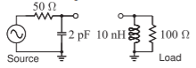
Figure \(\PageIndex{1}\)
- Design a Pi network to match the source configuration to the load configuration below. The design frequency is \(900\text{ MHz}\) and the desired \(Q\) is \(10\). [Parallels Example 10.6.2]
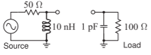
Figure \(\PageIndex{2}\)
- Develop the electrical design of an L-matching network to match the source to the load below.
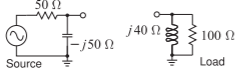
Figure \(\PageIndex{3}\)
- Develop the electrical design of an L-matching network to match the source to the load below.
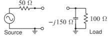
Figure \(\PageIndex{4}\)
- Design a lowpass lumped-element matching network to match the source and load shown below. The design frequency is \(1\text{ GHz}\). You must use a Smith Chart and clearly show your working and derivations. You must develop the final values of the elements.
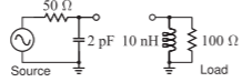
Figure \(\PageIndex{5}\)
- Consider the design of an L-matching network centered at \(100\text{ GHz}\) that will match a source with a Thevenin resistance of \(50\:\Omega\) to the input of an amplifier presenting a load resistance of \(200\:\Omega\) to the matching network. [Parallels Example 10.4.2 but note the DC blocking requirement below.]
- What is the \(Q\) of the matching network?
- The matching network must block DC current. Draw the topology of the matching network.
- What is the reactance of the series element in the matching network?
- What is the reactance of the shunt element in the matching network?
- What is the value of the series element in the matching network?
- What is the value of the shunt element in the matching network?
- Draw and label the final design of your matching network including the source and load resistance.
- Approximately, what is the \(3\text{ dB}\) bandwidth of the matching network?
- Design a two-element matching network to interface a source with a \(25\:\Omega\) Thevenin equivalent impedance to a load consisting of a capacitor in parallel with a resistor so that the load admittance is \(Y_{L} = 0.02 +\jmath 0.02\text{ S}\). Use the absorption method to handle the reactive load.
- Design a matching network to interface a source with a \(25\:\Omega\) Thevenin equivalent impedance to a load consisting of a capacitor in parallel with a resistor so that the load admittance is \(Y_{L} = 0.01 +\jmath 0.01\text{ S}\).
- If the complexity of the matching network is not limited, what is the minimum \(Q\) that could possibly be achieved in the complete network consisting of the matching network and the source and load impedances?
- Outline the procedure for designing the matching network for maximum bandwidth if only four elements can be used in the network. You do not need to design the network,
- Design a Pi network to match the source configuration to the load configuration below. The design frequency is \(900\text{ MHz}\) and the desired \(Q\) is \(10\).
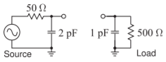
Figure \(\PageIndex{6}\)
- Design a passive matching network that will achieve maximum bandwidth matching from a source with an impedance of \(2\:\Omega\) (typical of the output impedance of a power amplifier) to a load with an impedance of \(50\:\Omega\). The matching network can have a maximum of three reactive elements. You need only calculate reactances and not the capacitor and inductor values.
- Design a passive matching network that will achieve maximum bandwidth matching from a source with an impedance of \(20\:\Omega\) to a load with an impedance of \(125\:\Omega\). The matching network can have a maximum of four reactive elements. You need only calculate reactances and not the capacitor and inductor values.
- Will you use two, three, or four elements in your matching network?
- With a diagram, and perhaps equations, indicate the design procedure.
- Design the matching network. It is sufficient to use reactance values.
- Design a passive matching network that will achieve maximum bandwidth matching from a source with an impedance of \(60\:\Omega\) to a load with an impedance of \(5\:\Omega\). The matching network can have a maximum of four reactive elements. You need only calculate reactances and not the capacitor and inductor values.
- Will you use two, three, or four elements in your matching network?
- With a diagram and perhaps equations, indicate the design procedure.
- Design the matching network. It is sufficient to use reactance values.
- Design a T network to match a \(50\:\Omega\) source to a \(1000\:\Omega\) load. The desired loaded \(Q\) is \(15\).
- Repeat Example 10.3.2 with an inductor in series with the load. Show that the inductance can be adjusted to obtain any positive shunt resistance value.
- Design a three-lumped-element matching network that interfaces a source with an impedance of \(5\:\Omega\) to a load with an impedance consisting of a resistor with an impedance of \(10\:\Omega\). The network must have a \(Q\) of \(6\).
- A two-port matching network is shown below with a generator and a load. The generator impedance is \(40\:\Omega\) and the load impedance is \(Z_{L} = 50 −\jmath 20\:\Omega\). Use a Smith chart to design the matching network.
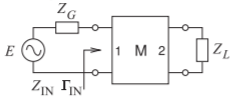
Figure \(\PageIndex{7}\)
- What is the condition for maximum power transfer from the generator? Express your answer using impedances.
- What is the condition for maximum power transfer from the generator? Express your answer using reflection coefficients.
- What system reference impedance are you going to use to solve the problem?
- Plot \(Z_{L}\) on the Smith chart and label the point. (Remember to use impedance normalization if required.)
- Plot ZG on the Smith chart and label the point.
- Design a matching network using only transmission lines. Show your work on the Smith chart. You must express the lengths of the lines in terms of electrical length (either degrees or wavelengths). Characteristic impedances of the lines are required. (You will therefore have a design that consists of one stub and one other length of transmission line.)
- Use a lossless transmission line and a series reactive element to match a source with a Thevenin equivalent impedance of \(25 +\jmath 50\:\Omega\) to a load of \(100\:\Omega\). (That is, use one transmission line and one series reactance only.)
- Draw the matching network with the source and load.
- What is the value of the series reactance in the matching network (you can leave this in ohms)?
- What is the length and characteristic impedance of the transmission line?
- Consider a load \(Z_{L} = 80 +\jmath 40\:\Omega\). Use the Smith chart to design a matching network consisting of only two transmission lines that will match the load to a generator of \(40\:\Omega\).
- Draw the matching network with transmission lines. If you use a stub, it should be a short-circuited stub.
- Indicate your choice of characteristic impedance for your transmission lines. What is the normalized load impedance? What is the normalized source impedance?
- Briefly outline the design procedure you will use. You will need to use Smith chart sketches.
- Plot the load and source on a Smith chart.
- Complete the design of the matching network, providing the lengths of the transmission lines.
- A two-port matching network is shown below with a generator and a load. The generator impedance is \(40\:\Omega\) and the load impedance is \(Z_{L} = 20 −\jmath 50\:\Omega\). Use a Smith chart to design the matching network.
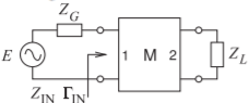
Figure \(\PageIndex{8}\)
- What is the condition for maximum power transfer from the generator? Express your answer using impedances.
- What is the condition for maximum power transfer from the generator? Express your answer using reflection coefficients.
- What system reference impedance are you going to use to solve the problem?
- Plot \(Z_{L}\) on a Smith chart and label the point. (Remember to use impedance normalization if required.)
- Plot \(Z_{G}\) on a Smith chart and label the point.
- Design a matching network using only transmission lines and show your work on a Smith chart. You must express the lengths of the lines in terms of electrical length (either degrees or wavelengths long). Characteristic impedances of the lines are required. (You will therefore have a design that consists of one stub and one other length of transmission line.)
- Use a Smith chart to design a microstrip network to match a load \(Z_{L} = 100 −\jmath 100\:\Omega\) to a source \(Z_{S} = 34 −\jmath 40\:\Omega\)). Use transmission lines only and do not use short-circuited stubs. Use a reference impedance of \(40\:\Omega\).
- Draw the matching network problem labeling impedances and the impedance looking into the matching network from the source as \(Z_{1}\).
- What is the condition for maximum power transfer in terms of impedances?
- What is the condition for maximum power transfer in terms of reflection coefficients?
- Identify, i.e. draw, at least two suitable microstrip matching networks.
- Develop the electrical design of the matching network using the Smith chart using \(40\:\Omega\) lines only. You only need do one design.
- Draw the microstrip layout of the matching network identify critical parameters such characteristic impedances and electrical length. Ensure that you identify which is the source side and which is the load side. You do not need to determine the widths of the lies or their physical lengths.
- Repeat exercise 24 but now with \(Z_{L} = 10−\jmath 40\:\Omega\) and \(Z_{S} = 28 −\jmath 28\:\Omega\)).
- Use a Smith chart to design a two-element lumped-element lossless matching network to interface a source with an admittance \(Y_{S} = 6 −\jmath 12\text{ mS}\) to a load with admittance \(Y_{L} = 70 −\jmath 50\text{ mS}\).
- Use a Smith chart to design a two-element lumped-element lossless matching network to interface a load \(Z_{L} = 50 +\jmath 50\:\Omega\) to a source \(Z_{S} = 10\:\Omega\).
10.12.1 Exercises by Section
\(†\)challenging
\(§10.3 1, 2\)
\(§10.4 3, 4\)
\(§10.5 5, 6, 7, 8, 9, 10, 11†, 12†, 13†\)
\(§10.6 14†, 15†, 16†, 17†, 18†, 19†\)
\(§10.7 20†, 21†, 22†, 23†\)
\(§10.9 24, 25, 26, 27\)
10.12.2 Answers to Selected Exercises
- (c) \(Q=1.22467\)
- \(C=1/(\omega_{d}^{2}L_{P})\)
- (d) \(1.25-\jmath 0.5\)
- (b) \(-\jmath 50\:\Omega\)
- (f) \(40\:\Omega\), \(0.085\) \(\lambda\)-long line before load, \(40\:\Omega\), \(0.076\) \(\lambda\)-long shorted stub