
11.12: Switch
- Page ID
- 41346

In many cellular systems a phone does not transmit and receive simultaneously. Consequently a switch can be used to alternately connect a transmitter and a receiver to an antenna. An ideal switch is shown in Figure \(\PageIndex{1}\)(a), where an input port, \(\text{RF}_{\text{IN}}\), and an output port, \(\text{RF}_{\text{OUT}}\), are shown. At microwave frequencies, realistic switches must be modeled with parasitics and with finite on and off resistances. A realistic model applicable to many switch types is shown in Figure \(\PageIndex{1}\)(b). The capacitive parasitics, the \(C_{P}\text{s}\), limit the frequency of operation and the on resistance, \(R_{\text{ON}}\), causes loss. Ideally the off resistance, \(R_{\text{OFF}}\), is very large, however, the parasitic shunt capacitance, \(C_{\text{OFF}}\), is nearly always more significant. The result is that
| Switch type | Power handling | Insertion loss | Operating frequency | Actuation voltage | Response time |
|---|---|---|---|---|---|
| MEMS\(^{1}\) | \(0.5\text{ W}\) | \(0.5\text{ dB}\) | to \(10\text{ GHz}\) | \(90\text{ V}\) | \(10\:\mu\text{s}\) |
| MEMS\(^{1}\) | \(4\text{ W}\) | \(0.8\text{ dB}\) | to \(35\text{ GHz}\) | \(110\text{ V}\) | \(10\:\mu\text{s}\) |
| pHEMT\(^{2}\) | \(10\text{ W}\) | \(0.3\text{ dB}\) | to \(6.5\text{ GHz}\) | \(5\text{ V}\) | \(0.5\:\mu\text{s}\) |
| pHEMT\(^{2}\) | \(0.3\text{ W}\) | \(1.1\text{ dB}\) | to \(25\text{ GHz}\) | \(5\text{ V}\) | \(0.5\:\mu\text{s}\) |
| PIN\(^{3}\) | \(13\text{ W}\) | \(0.35\text{ dB}\) | to \(2\text{ GHz}\) | \(12\text{ V}\) | \(0.5\:\mu\text{s}\) |
| PIN\(^{3}\) | \(10\text{ W}\) | \(0.4\text{ dB}\) | to \(6\text{ Hz}\) | \(12\text{ V}\) | \(0.5\:\mu\text{s}\) |
Table \(\PageIndex{1}\): Typical properties of small microwave switches. (Sources: \(^{1}\)Radant MEMS, \(^{2}\)RF Micro Devices, and \(^{3}\)Tyco Electronics.)
at high frequencies there is an alternative capacitive connection between the input and output through COFF. The on resistance of the switch introduces voltage division that can be seen by comparing the ideal connection shown in Figure \(\PageIndex{1}\)(c) and the more realistic connection shown in Figure \(\PageIndex{1}\)(d). There are four main types of microwave switches: mechanical (rarely used except in instrumentation), PIN diode, FET, and microelectromechanical system (MEMS), see Figures \(\PageIndex{1}\)(e–g) and Table \(\PageIndex{1}\).
A MEMS switch is fabricated using photolithographic techniques similar to those used in semiconductor manufacturing. They are essentially miniature mechanical switches with a voltage used to control the position of a shorting arm, see Figure \(\PageIndex{2}\).
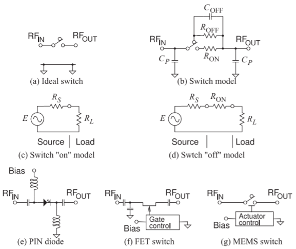
Figure \(\PageIndex{1}\): Microwave switches: (a) ideal switch connecting \(\text{RF}_{\text{IN}}\) and \(\text{RF}_{\text{OUT}}\) ports; (b) model of a microwave switch; (c) ideal circuit model with switch on and with source and load; (d) realistic low-frequency circuit model with switch on; (e) switch realized using a PIN diode; (f) switch realized using an FET; and (g) switch realized using a MEMS switch.
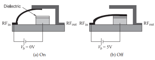
Figure \(\PageIndex{2}\): RF MEMS switch: (a) the \(\text{RF}_{\text{in}}\) line in contact with the \(\text{RF}_{\text{out}}\) line; and (b) the cantlever beam electrostatically attracted to the pedestal and there is no RF connection.
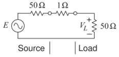
Figure \(\PageIndex{3}\): Model used in calculating the loss of a switch in a \(50\:\Omega\) system.
Example \(\PageIndex{1}\): Insertion Loss of a Switch
What is the insertion loss of a switch with a \(1\:\Omega\) on resistance when it used in a \(50\:\Omega\) system?
Solution
The model to be used for evaluating the insertion loss of the switch is shown in Figure \(\PageIndex{3}\). The insertion loss is found by first determining the available power from the source and then the actual power delivered to the load. The available input power is calculated by first ignoring the \(1\:\Omega\) switch resistance. Then there is maximum power transfer from the source to the load. The available input power is
\[\label{eq:1}P_{Ai}=\frac{1}{2}\frac{(\frac{1}{2}E)^{2}}{50}=\frac{E^{2}}{400} \]
where \(E\) is the peak RF voltage at the Thevenin equivalent source generator. The power delivered to the \(50\:\Omega\) load is found after first determining the peak load voltage:
\[\label{eq:2}V_{L}=\frac{50}{50+1+50}E=\frac{50}{101}E \]
Thus the power delivered to the load is
\[\label{eq:3}P_{D}=\frac{1}{2}\frac{V_{L}^{2}}{50}=\frac{1}{100}\left(\frac{50}{101}\right)^{2}E^{2} \]
The insertion loss is
\[\label{eq:4}\text{IL}=\frac{P_{Ai}}{P_{D}}=\frac{E^{2}}{400}\frac{100}{E^{2}}\left(\frac{101}{50}\right)^{2}=1.020=0.086\text{ dB} \]