
1.1: Basic Components in a CPU
- Page ID
- 27161

This section covers the basic components in a CPU. It covers the gates which are used in the CPU, and four common ICs used in a CPU, the adder, decoder, multiplexer, and register.
1.1.1 Boolean operations
Gates are hardware implementations of Boolean operations. Boolean operations are operations that take one or more binary values and calculate a result. For example, the AND operation takes 2 binary value (with 0 = false and 1 = true) and calculates a binary output. For the AND operations, the inputs of 0 AND 0, 0 AND 1, and 1 AND 0 all yield 0 (false), and the input of 1 AND 1 yields 1 (true). This is normally implemented using a truth table, as follows:
|
Input |
Output |
|
|
A |
B |
AND |
| 0 | 0 | 0 |
| 0 | 1 | 0 |
| 1 | 0 | 0 |
| 1 | 1 | 1 |
In this text 5 Boolean operators will be used, the AND, OR, NOT, XOR, and NAND. The NOT is a unary function (it only takes one input), and so is given in Table 1-2.
|
Input |
Output |
|
A |
NOT |
| 0 | 1 |
| 1 | 0 |
The AND, OR, XOR, and NAND operators are binary (taking two inputs) and shown in Table 1- 3 below.
|
Input |
Output |
||||
|
A |
B |
AND |
OR |
XOR |
NAND |
| 0 | 0 | 0 | 0 | 0 | 1 |
| 0 | 1 | 0 | 1 | 1 | 1 |
| 1 | 0 | 0 | 1 | 1 | 1 |
| 1 | 1 | 1 | 1 | 0 | 0 |
1.1.2 Integrated Circuits
An Integrated Circuit (IC) is a collection of gates that are used to build components to implement a behavior. The components of an IC are simple gates, and all of the ICs in this chapter can be reduces easily to AND, OR, NOT, XOR, and NAND gates. So just as the gates mechanically transform input into output, the ICs also do a mechanical transformation of inputs into outputs.
The ICs to be described in this chapter are the Adder, Decoder, Multiplexer, and Flip Flop.
1.1.3 ALU (Adder)
The Arithmetic Logic Unit (ALU) is the central component of the CPU. It performs all arithmetic and logical operations on the data. Everything else in the CPU is designed to provide data for the ALU to operate on.
The ALU is normally a black box that provides the operations for the CPU on two operands. This black box is responsible for all operations that the CPU performs, including not only integer and logical operations, but floating point calculations as well. Operations like floating point calculations are very complex, and are often implemented in coprocessors. To keep things simple, the only data types allowed for the CPU in this text will be integers, and only integer and logic operations will be allowed.
An overview of an ALU can be seen in the typical ALU shown below. An ALU takes two arguments, and implements and operation, such as add, subtract, multiply and divide operations on these two operands. The ALU also allows operations such as Boolean operations (AND, OR, XOR, etc), bit-shifting, and comparison.

Because the only ALU operation covered in the recommended text on ICs is an adder, the ALU the used in the Logisim implementation of the CPU will contain only an adder circuit. Using an adder, both addition and subtraction are implemented. A more robust configuration for an ALU is can be found in the extra notes that can be accessed for this text.
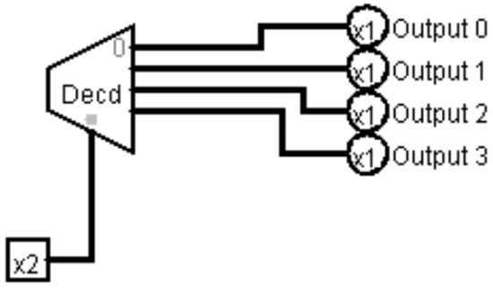
1.1.4 Decoder
A decoder is an IC splits a n-bit number into 2n separate output lines. For example, consider a 2- bit number, which can have 4 values, 0x0 ... 0x3. A decoder would take as input 2 input lines representing the 2-bit number, and turn on one (and only one) of the four output lines. The line which is turned on corresponds to the value of the 2-bit input. So in the following diagram, if the 2-bit input has both lines high (representing “11”), and the output line 3 is turned on.
1.1.5 Multiplexer
A multiplexer is an IC that selects between different inputs. In the following diagram, the 8 bits used by the Output can come from either Register 1 or Register 2. The MUX selects which 8-bit value to use. If Select Input is 0, Register 1 is chosen, and if Select Input is 1 Register 2 is chosen.

1.1.6 Registers (D Flip Flops) and Memory
Memory is different than the other ICs in that it is synchronous, where synchronous means the memory cell has a value which at discrete time intervals. An example of this behavior is the $ac in the following program fragment:
clac    <- time = t0, $ac = 5
addi 5  <- time = t1, $ac = 5
addi 7  <- time = t2, $ac = 5
subi 2  <- time = t3, $ac = 5
This program shows that the value of the memory, $ac, changes discretely over time. This discrete behavior is accomplished by a system clock. A system clock is an electronic oscillator circuit that produces a square wave with a precise frequency. The following is an illustration of a square wave.

In a square wave, the value is always 0 or 1, and memory uses the transition from 0 to 1 (the positive edge) to change the value of all memory components. Thus memory cells have discrete values that change on each clock pulse.
Any memory cell in a CPU is normally called a register. Register memory normally consists of Static Ram (SRAM), and is implemented using Flip Flops. Main computer memory is often Dynamic Ram (DRAM)., however some memory, particularly cache memory, can be implemented with SRAM. The specifics of memory are beyond the scope of this text, and the all the reader needs to know is register memory is most typically SRAM and located within the CPU.