
2.1: Procedure
- Page ID
- 26463

After logging into the computer, open TINA. If a desktop shortcut is not available TINA may be accessed via the Programs menu under the TINA menu item. You will be greeted with something similar to the screen shown in Figure \(\PageIndex{1}\). Depending on the version, the precise look of the program may be a little different from that shown (TINA-TI). There are two toolbar strips immediately below the menus. The topmost toolbar contains the usual File Open, Save, and similar commands, along with buttons for text insertion, zoom level and the like. At the extreme right end of this strip is search box for electronic components. The lower strip is made up of a set of tabbed toolbars for electronic components, measurement instruments and other devices. Selecting a given tab (e.g., Basic, Meters, Semiconductors, etc.) shows the toolbar for that set of items.
TINA’s schematic capture facility is object based, that is, you “draw” a circuit by selecting predefined objects such as resistors and transistors, and drag them onto the workspace. They are then wired together using the mouse. You can zoom into or out of the workspace using the mouse or the zoom toolbar button.
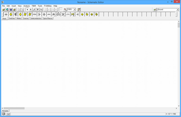
Figure \(\PageIndex{1}\)
TINA will draw schematics using one of three formats. The first style uses the ANSI (North American) standard for schematic symbols. The second style uses the DIN (Euro) standard. The final style is called "3D" where components look more like photographs of the actual component. Examples are shown in Figure \(\PageIndex{2}\) using ANSI, DIN and 3D. You can set the preferred format via the View->Options menu item. More on this in a moment.
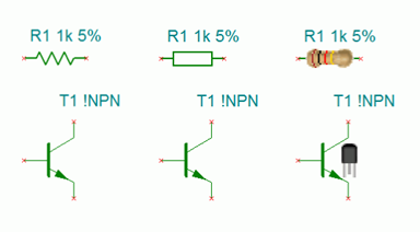
Figure \(\PageIndex{2}\)
Generally, we do not use the 3D style for most work. It is, however, useful for newcomers as a way of reinforcing and practicing use of the resistor color code, and for general package identification (such as the TO-92 transistor case pictured in Figure \(\PageIndex{2}\)). TINA will show the proper color sequence for resistors using either two or three significant digits along with a proper tolerance band (i.e., four or five bands). A comparison is shown in Figure \(\PageIndex{3}\).
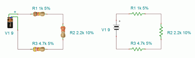
Figure \(\PageIndex{3}\)
Along with the appropriate electronic parameters of a device, physical data regarding shape and pinout are required if a printed circuit board (PCB) will be created. For example, a particular device such as an operational amplifier may be available in several different package styles including through-hole or surface mount variants. Our goal here is to become familiar with capturing the schematic and performing simulations, such as verifying a laboratory exercise. Consequently, we shall not concern ourselves with the needs of PCB layout at this point.
To illustrate the use and editing of components, select the Basic tab and drag a DC voltage source (third item) onto the workspace. It will show up with a default voltage value and label. Double click the symbol. A dialog box will pop up next to it as shown in Figure \(\PageIndex{4}\).
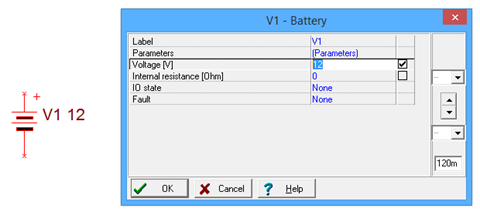
Figure \(\PageIndex{4}\)
From this dialog you can change a variety of attributes, the most important of which are the voltage value and the label. Double clicking any component will bring up a settings dialog box although the precise items contained within it will vary from component to component. For example, for a resistor there will be a resistance setting instead of a voltage setting. If you need to remove a component, simply select it and hit the Delete key.
Electronic components can be placed into two broad categories; generic parts and more accurate "real world" models typically generated by the manufacturer of that part. This is particularly true with complex components or devices. For example, Figure \(\PageIndex{5}\) shows a pair of NPN transistors. The one labeled "!NPN" is a simple generic model. The lower, highlighted transistor references a specific part number, in this case the 2N3904, a popular general purpose device.
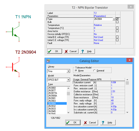
Figure \(\PageIndex{5}\)
Double clicking the generic transistor opens up its settings dialog box. Initially, under Type, it will say "NPN", referring to the generic. Next to this is a small box labeled with an ellipsis (...). Clicking on the ellipsis will open a second settings box, the Catalog Editor. From here, a specific manufacturer's part can be selected from the scrolling list on the left. If need be, specific parameters can be altered in the list on the right.
Remember, whenever you see the small ellipsis box, clicking on it will open another settings box so that you can specify further details.
Editing the position and orientation of a component is straightforward. Once the item is selected (highlighted in red by default) it may be moved using either the mouse or the cursor keys. If you need to move a group of components, the mouse may be used to select several items by clicking and then dragging the mouse over them. Every component within the selection box will be highlighted and will move as a group. Components may also be rotated and flipped. These commands can be accessed from the main menu, however, it is handy to remember certain keyboard shortcuts (such as Ctrl-R for rotate right, or clockwise). Also note that it is possible to select the text labels of components and move or rotate them independently of the component. This can be handy if a label becomes obscured by a wire. To do so, make sure the component is not selected (unhighlighted) and then click directly on the label. It can now be moved or rotated.
Along with editing the components, you may also customize the look of the work space. From the file menu, select Page Setup. This opens the dialog box shown in Figure \(\PageIndex{6}\) and allows you to specify the sheet size for the schematic and related properties.
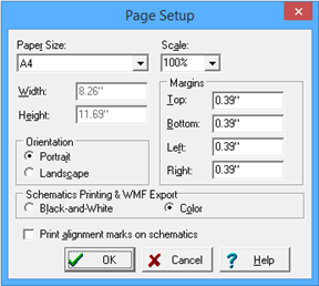
Figure \(\PageIndex{6}\)
Other attributes, such as whether or not to show the grid, component values, labels, and the like can be selected from the View menu. This is shown in Figure \(\PageIndex{7}\). Of particular importance is the final item in this list, Options, which was mentioned earlier. Selecting Options brings up the Editor settings box shown in Figure \(\PageIndex{8}\).
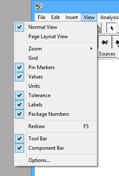
Figure \(\PageIndex{7}\)
The Editor options include the aforementioned ANSI, DIN and 3D styles. It also includes the base function for AC (it is recommended this be set to sine). Further, you can adjust the color scheme for your workspace and a few other global parameters.
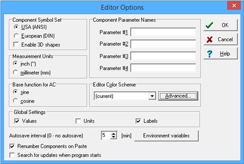
Figure \(\PageIndex{8}\)
OK, let’s create a circuit and perform a simulation. If you have been experimenting, remove any components on your workspace (select with the mouse and then press the Delete key). From the Basic components tab, select a DC voltage source, two resistors and an earth ground symbol. We shall make a series loop of the three elements with the negative end of the power supply at ground. One resistor will need to be rotated 90 degrees (one horizontal and one vertical). In order to wire the items together, move the mouse to the end of one component you wish to wire. The connection ends are denoted with a small red x. When the mouse cursor is close, it will turn into a pen shape. Simply click on the lead of the component and move the mouse to the desired lead of another component. While moving, TINA will draw a red line. Clicking on the second component will create a proper wire (by default, colored black). Wires are always drawn along the horizontal and vertical with 90 degree bends, not directly from point to point. This is the proper way to draw a schematic in the vast majority of cases.
To delete a wire, click on it to select it. You will see a set of small “handles” on it. To remove the wire, simply hit the Delete key.
Note that you can also move the wire with those handles if desired. Note that if you move a component, TINA will automatically move the wires along with it. You do not have to rewire it. If a component is later deleted, this will result in "dangling wires" which also should be deleted.
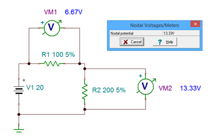
Figure \(\PageIndex{9}\)
Once the components are in place and wired, double-click each component to set their values as shown in Figure \(\PageIndex{9}\). We shall then add two the two voltmeters (fifth item in the Basic tab). Please note that it is perfectly acceptable to change the component values immediately after dragging them onto the work space; you don’t have to wait until they are wired together. It is suggested, though, that you decide upon a particular workflow and stick to it otherwise the chances of forgetting to change components from their default values increases.
The circuit is now ready to perform a simulation.
From the Analysis menu, select DC Analysis->Calculate nodal voltages. In a moment, the values of the voltages will be printed next to the voltmeters. Also, a small window will pop up. With this window, you can investigate particular node voltages or component voltages and currents. You will notice that the mouse cursor will have changed shape into a measurement probe. You can click on a node to see a voltage with respect to ground (a node is denoted with a small, solid black circle on the wire where items connect, such as where a meter connects to a wire). Further, if you click on a component, the voltage across it and the current through it will be displayed in the little pop up window. This is a nice interactive feature.
TINA also has a wide variety of virtual instruments. These can be accessed via the T&M (Test and Measurement) menu. For example, Figure \(\PageIndex{10}\) illustrates a virtual oscilloscope. This has the advantage of immediacy (assuming you’ve used an oscilloscope before), however, it is not the ultimate way to perform a simulation. We will look at even more powerful and flexible ways of creating simulations in the next exercise.
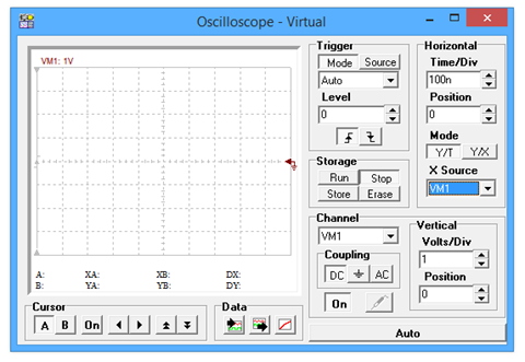
Figure \(\PageIndex{10}\)
For now, you may wish to delete this new instrument from the work space and then save the existing schematic. Remember to always save to either your student account or to a USB drive. Never save directly to the hard drive in lab.
There are three very good “every day” uses for TINA during your studies: First, it is a very handy tool for verifying lab results. That is, you can recreate a lab circuit, simulate it, and compare the simulation to both your theoretical calculations and lab measurements. Second, it is a handy tool for checking homework if you get stuck on a problem. Third, it is convenient for the creation of schematics, for example, for a lab report. An easy way to do this is to draw the circuit, capture the screen image (Windows key+Print Screen key copies it into the clipboard) and then paste the image into your favorite image manipulation program. From there you can crop it, change contrast, etc. as needed and then paste the modified image into your lab report.
At this point you may wish to experiment a bit by rewiring the circuit or to try building new circuits. As with any tool, continued practice will hone your skill. Once you are done and have saved the file (the extension should be .TSC), close TINA and then shut down the computer.