
1.4: Doped Materials
- Page ID
- 25309

By themselves, intrinsic semiconductors are not of particular use. They are neither good conductors nor insulators, and their conduction is largely dependent on temperature. We can alter the properties of the material by introducing foreign substances or impurities into the crystal. These impurities are also known as dopants. A crystal with an added dopant is referred to as an extrinsic semiconductor or doped material. The amount of impurity added is generally small, perhaps in the neighborhood of one part per million. The dopant may be added through a gaseous diffusion process where the crystal is heated in an oven and the dopant added in gaseous form. Over a period of time the impurities will diffuse or “seep into” the target crystal. An alternate approach is ion implantation. In this method the impurities are accelerated and quite literally smash into the target, dislodging and replacing some of the original atoms in the crystal.
There are two different types of semiconductors possible. One is called N-type material, and the other, P-type material. Unsurprisingly, the N stands for Negative and the P stands for (you guessed it) Positive. N-type material is created by adding pentavalent impurities, that is, a dopant with five electrons in its outer shell. Examples include phosphorus, arsenic and antimony. In contrast, P-type material is created by adding a trivalent impurity, one with three electrons in its outer shell. Possible trivalent impurities include boron, gallium and indium.
1.4.1: N-Type Material
Figure \(\PageIndex{1}\) shows a model of a silicon crystal with a pentavalent impurity at its center. Compared to an ordinary silicon atom that would have four electrons in its outer shell, the pentavalent impurity creates an extra, or donor, electron. Thus, the crystal has a net negative charge and is referred to as N-type material. The energy level of the donor electrons is just below the bottom of the conduction band. In other words, the difference between the donor level and the bottom of the conduction band is much, much smaller than the band gap itself. Therefore it is relatively easy for these donor electrons to jump into the conduction band, becoming free ionized electrons and leaving behind ionized holes1.
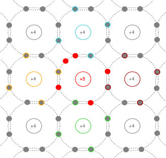
Figure \(\PageIndex{1}\): Crystal with added pentavalent impurity (N-type).
Compared to the undoped intrinsic crystal, the doped extrinsic crystal exhibits a relatively high number of free electrons. As you might surmise, this enhances the conductivity of the material, and the greater the doping level, the greater the enhancement. Earlier it was mentioned that both electrons and holes can serve as charge carriers. Because the number of free electrons is significantly larger than the number of holes in N-type material, electrons in N-type material are referred to as the majority charge carrier (or more simply, the majority carrier) while holes are referred to as the minority charge carrier (or minority carrier).
The extra electrons add to the number of filled energy states and, being of higher energy than the valence electrons, push the Fermi level to a higher value. Remember, the Fermi level represents the point where 50% of states would be filled, so if we add states above this, then the new 50% point must be higher than the former level. This is illustrated in Figure \(\PageIndex{2}\). Note how close the donor level is to the conduction band and that the Fermi level has been pushed up, away from the valence band and closer to the conduction band. This will be of great significance in up-coming discussions on semiconductor devices.
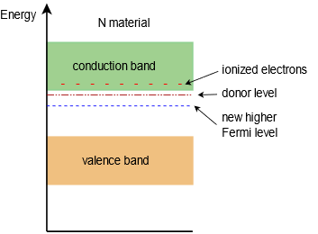
Figure \(\PageIndex{2}\): Energy band diagram of N-type semiconductor.
1.4.2: P-Type Material
In a similar manner, if we introduce a trivalent impurity, our crystal model now features a hole; a location where an electron is lacking. For this reason, trivalent impurities are sometimes called acceptors. The resulting crystal model is illustrated in Figure \(\PageIndex{3}\).
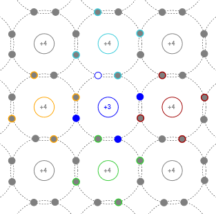
Figure \(\PageIndex{3}\): Crystal with added trivalent impurity (P-type).
The resulting situation is essentially the reverse of that of the N-type material. Figure \(\PageIndex{4}\) shows the energy band diagram for our new P-type material. In this case, the Fermi level has been pushed down, closer to the valence band.
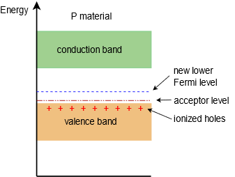
Figure \(\PageIndex{4}\): Energy band diagram of Ptype semiconductor.
In P-type material, holes out number free electrons. Consequently, holes are referred to as the majority carrier in P material while electrons take on the role of minority charge carrier.
As with N-type material, the greater the amount of trivalent impurity added, the greater the overall effect. By itself, a doped crystal can be used to create a resistor. The resistivity of the material is a function of the doping level. By setting the cross-sectional area, length and doping level, we can create well-defined resistor values. If this was all we could do with semiconductors then we could say two things: first, the solid state semiconductor revolution would not exist; and second, this text would be very short. The interesting bits arrive when we combine both N- and P-type materials into a single device, as we shall begin to see in the next chapter.
References
1An ion is an atom or molecule that does not have a neutral net charge, i.e., the numbers of protons and electrons are not equal. If it loses electrons, resulting in a net positive charge, it is called a cation. If it gains electrons resulting in a net negative charge it is called an anion.