
7.3: Common Emitter Amplifier
- Page ID
- 25426

The common emitter configuration finds wide use as a general purpose voltage amplifier. We begin with a basic DC biasing circuit and then add a few other components. For example, refer to Figure \(\PageIndex{1}\).
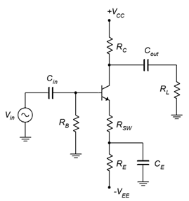
Figure \(\PageIndex{1}\): Common emitter amplifier using two-supply emitter bias.
This amplifier is based on a two-supply emitter bias circuit. The notable changes are the inclusion of an input signal voltage, \(V_{in}\), and a load, \(R_L\). So that these components do not alter the bias, we isolate the input and load through the use of coupling capacitors \(C_{in}\) and \(C_{out}\). These capacitors will act as opens to DC creating the desired isolation. As for the AC signal, the capacitances will be chosen such that their reactances will be much smaller than the surrounding resistors at the frequency of the input. Consequently, the capacitors will appear as shorts and allow the AC signal to pass through the amplifier.
The final alteration involves the emitter resistor. The single resistor of the bias network is replaced by a pair of resistors, \(R_E\) and \(R_{SW}\), along with a bypass capacitor, \(C_E\). For DC, the capacitor is open and the effective emitter bias resistance is \(R_E + R_{SW}\). For AC, the capacitor will behave ideally as a short so the AC emitter resistance will fall to just \(R_{SW}\). This resistor is called a swamping or emitter degeneration resistor. It is used primarily to help control the voltage gain of the amplifier.
We can use our AC transistor model along with the Superposition Theorem to arrive at an equivalent AC circuit of the amplifier, as shown in Figure \(\PageIndex{2}\).
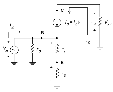
Figure \(\PageIndex{2}\): AC equivalent of common emitter amplifier.
First, we have shorted all of the capacitors. Second, we have replaced the DC sources with their ideal internal resistance (a short) which places those points at AC ground. Third, we swapped out the transistor for the model. Lastly, we have combined and/or renamed resistances where needed. Because this is an AC circuit, we use the convention of lower case \(r\) for resistance to avoid confusion with the DC resistance (which are upper case). Thus, \(r_E\) is the AC resistance from the emitter to AC ground. This corresponds to \(R_{SW}\) in the original schematic. Similarly, \(r_C\) represents the total resistance seen from the collector to AC ground. In the original schematic this corresponds to \(R_C\) in parallel with \(R_L\). If this circuit was unloaded, then \(r_C\) would just be equal to \(R_C\). Finally, \(r_B\) corresponds to \(R_B\) but in a voltage divider bias it would be equal to \(R_1\) in parallel with \(R_2\).
7.3.1: Voltage Gain
Voltage gain, \(A_v\), is defined as the ratio of \(v_{out}\) to \(v_{in}\). Using Ohm's law we find
\[A_v = \frac{v_{out}}{v_{i n}} = \frac{v_C}{v_B} \\ A_v = \frac{−i_C r_C}{i_C (r'_e+r_E ) } \\ A_v =− \frac{r_C}{r'_e+r_E} \label{7.4} \]
First, the negative sign indicates that this amplifier inverts the waveform, top to bottom. For a sine wave, this is equivalent to shifting the phase 180\(^{\circ}\). In some applications this can be a major issue, in others, not so much. If it is an issue, it can be resolved by using a second inverting gain amplifier in sequence with the first (inverting the inversion).
The second thing we see is that the gain is little more than a ratio of collector to emitter resistances. This is where splitting the emitter resistor into two parts comes in. In the equation, \(r_E\) is the swamping resistor \(R_{SW}\). The larger the swamping resistor, the lower the gain. The maximum gain will be achieved when \(R_{SW} = 0\). That is, when the emitter is completely bypassed. The down side of this is that the gain will now depend entirely on \(r'_e\). This will increase the distortion. The reason is because \(R_{SW}\), being so much larger, effectively “swamps out” the variation in \(r'_e\) and reduces distortion. The larger \(R_{SW}\) is relative to \(r'_e\), the greater the reduction in distortion, but with the cost of reduced gain. This is why a swamping resistor is also called an emitter degeneration resistor: it degrades the voltage gain.
7.3.2: Input Impedance
Input impedance, \(Z_{in}\), is defined as the ratio of \(v_{in}\) to \(i_{in}\). In Figure 7.2.2 this is equal to \(r_B\) in parallel with the impedance looking into the base terminal, \(Z_{in(base)}\). Using Ohm's law we find
\[Z_{i n(base)} = \frac{v_B}{i_B} \\ Z_{i n(base)} = \frac{i_C (r'_e+r_E )}{i_B} \\ Z_{i n(base)} = \frac{i_C (r'_e+r_E )}{i_C / \beta} \\ Z_{i n(base)} = \beta (r'_e+r_E ) \label{7.5} \]
Therefore
\[Z_{in} = r_B || Z_{in(base)} \label{7.6} \]
We see that both the swamping resistor and \( \beta \) play a role in setting the input impedance. Larger values of \(R_{SW}\) and \( \beta \) produce larger input impedances. In sum, we find that while swamping decreases voltage gain, it reduces distortion and increases input impedance, the latter two generally desirable for a voltage amplifier. A non-swamped amplifier will have the largest gain but will suffer from the worst distortion and a low input impedance. This is a classic “quality versus quantity” trade-off: a large low quality gain versus a modest high quality gain1.
7.3.3: Output Impedance
Output impedance, \(Z_{out}\), is defined as the internal impedance of the equivalent source that drives the load. If we position ourselves at the load and look back into the amplifier shown in Figure 7.2.1, \(C_{out}\) is shorted ideally and \(V_{CC}\) is at AC ground. This leaves us with \(R_C\) in parallel with the transistor. The transistor is modeled as a current source and its ideal internal resistance would approach infinity. In reality, the effective value, \(r'_C\), is likely in the region of 100 k\( \Omega \) or so, depending on bias current. This parallel combination comprises the output impedance of the current source. We model this circuit as a voltage amplifier so to be proper, we'd convert the current source with parallel internal resistance to a voltage source with series internal resistance. Those resistance values are identical, though, and we arrive at
\[Z_{out} = r'_C || R_C \nonumber \]
In many circuits, \(R_C\) is considerably smaller than \(r'_C\), therefore
\[Z_{out} \approx R_C \label{7.7} \]
Example \(\PageIndex{1}\)
Determine the input and output impedances of the amplifier shown in Figure \(\PageIndex{3}\). Also compute the voltage gain. Assume \( \beta = 150\).
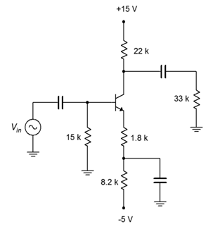
Figure \(\PageIndex{3}\): Schematic for Example \(\PageIndex{1}\).
First, the easy bit. We can determine the output impedance by inspection. It is approximately equal to \(R_C\), or 22 k\( \Omega \).
In order to find \(Z_{in}\) and \(A_v\), we will need to determine \(r'_e\). To obtain \(r'_e\) we need to find \(I_C\). Using KVL around the base-emitter loop, if we approximate the DC base voltage to be near zero, then all of the emitter supply drops across the DC emitter resistance, with the exception of \(V_{BE}\).
\[I_C = \frac{∣V_{EE}∣−V_{BE}}{R_E+R_{SW}} \nonumber \]
\[I_C = \frac{5 V−0.7 V}{8.2 k \Omega +1.8 k \Omega} \nonumber \]
\[I_C = 0.43 mA \nonumber \]
\[r'_e = \frac{26mV}{I_C} \nonumber \]
\[r'_e = \frac{26mV}{0.43 mA} \nonumber \]
\[r'_e = 60.5 \Omega \nonumber \]
\[Z_{i n−base} = \beta (r'_e+r_E ) \nonumber \]
\[Z_{i n−base} = 150(60.5 \Omega +1.8k \Omega ) \nonumber \]
\[Z_{i n−base} = 279 k \Omega \nonumber \]
This value in parallel with the base biasing resistor creates the input impedance.
\[Z_{i n} = R_B || Z_{i n(base)} \nonumber \]
\[Z_{i n} = 15k \Omega || 279 k \Omega \nonumber \]
\[Z_{i n} = 14.2k \Omega \nonumber \]
First, method one.
\[r_C = R_C || R_L \nonumber \]
\[r_C = 22 k \Omega || 33 k \Omega \nonumber \]
\[r_C = 13.2 k \Omega \nonumber \]
\[A_v =− \frac{r_C}{r'_e+r_E} \nonumber \]
\[A_v =− \frac{13.2 k \Omega}{ 60.5 \Omega +1.8 k \Omega} \nonumber \]
\[A_v =−7.1 \nonumber \]
And now method two; first the unloaded gain, then the divider effect and finally, the composite gain.
\[A_{v ( unloaded )} =− \frac{r_C}{r'_e+r_E} \nonumber \]
\[A_{v ( unloaded ) } =− \frac{22 k \Omega}{60.5 \Omega +1.8 k \Omega} \nonumber \]
\[A_{v ( unloaded )} =−11.82 \nonumber \]
\[A_{divider} = \frac{R_L}{R_L+R_C} \nonumber \]
\[A_{divider} = \frac{33 k \Omega}{33k \Omega +22k \Omega} \nonumber \]
\[A_{divider} = 0.6 \nonumber \]
\[A_v = A_{v (unloaded )} \times A_{divider} \nonumber \]
\[A_v =−11.82 \times 0.6 \nonumber \]
\[A_v =−7.1 \nonumber \]
We shall repeat the prior example using the same circuit but with one change: the emitter resistor will be completely bypassed. This will show the effect that swamping has on voltage gain and input impedance.
Example \(\PageIndex{2}\)
Determine the voltage gain and input impedance of the amplifier shown in Figure \(\PageIndex{4}\). Assume \( \beta = 150\).
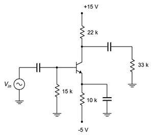
Figure \(\PageIndex{4}\): Schematic for Example \(\PageIndex{2}\).
The DC equivalent of this circuit is identical to that of the circuit shown in Figure \(\PageIndex{3}\). In both cases, the DC emitter resistance is 10 k\( \Omega \). Therefore, \(I_C\) and \(r'_e\) are unchanged. The bypass capacitor shorts this entire value for the AC equivalent because there is no swamping resistor. Consequently, \(r_E\) = 0. We can simply use 0 for \(r_E\) in the equations previously derived.
We begin with the input impedance.
\[Z_{i n−base} = \beta (r'_e+r_E ) \nonumber \]
\[Z_{i n−base} = 150(60.5 \Omega +0) \nonumber \]
\[Z_{i n−base} = 9075 \Omega \nonumber \]
This value is considerably smaller than the value obtained from the swamped circuit. Continuing,
\[Z_{i n} = R_B || Z_{i n(base)} \nonumber \]
\[Z_{i n} = 15k \Omega ∣∣ 9075 \Omega \nonumber \]
\[Z_{i n} = 5654 \Omega \nonumber \]
\[A_v =− \frac{r_C}{r'_e+r_E} \nonumber \]
\[A_v =− \frac{13.2 k \Omega}{60.5 \Omega +0 } \nonumber \]
\[A_v =−218.2 \nonumber \]
The end result is an input impedance less than half of the swamped case and a voltage gain over 30 times greater. What these calculations do not show is the increase in distortion that will be created by this change. More on that in a moment.
Let's consider something slightly different: a voltage divider bias PNP amplifier.
Example \(\PageIndex{3}\)
Determine the input impedance and voltage gain for the circuit shown in Figure \(\PageIndex{5}\). Also determine \(v_{load}\) if \(v_{in}\) = 20 mV peak. Assume \( \beta = 100\).
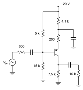
Figure \(\PageIndex{5}\): Schematic for Example \(\PageIndex{3}\).
We need to first determine \(r'_e\) which means that we need to find the collector current. If we assume a lightly loaded divider, the base voltage will be approximately 15 volts and the emitter will be 0.7 volts higher, or 15.7 volts. This leaves 20 volts − 15.7 volts, or 4.3 volts, across the DC equivalent emitter resistance. That's 4.1 k \( \Omega \) + 200 \( \Omega \), or 4.3 k\( \Omega \), yielding 1 mA for \(I_C\). This will produce \(r'_e\) = 26 \( \Omega \).
\[Z_{i n(base)} = \beta (r'_e+r_E ) \nonumber \]
\[Z_{i n(base)} = 100(26 \Omega +200 \Omega ) \nonumber \]
\[Z_{i n(base)} = 22.6 k \Omega \nonumber \]
This value is in parallel with the voltage divider biasing resistors, creating the input impedance.
\[Z_{i n} = R_1 || R_2 || Z_{i n(base )} \nonumber \]
\[Z_{i n} = 15k \Omega || 5k \Omega || 22.6 k \Omega \nonumber \]
\[Z_{i n} = 3.22 k \Omega \nonumber \]
\[A_v =− \frac{r_C}{r'_e+r_E} \nonumber \]
\[A_v =− \frac{7.5k \Omega || 10 k \Omega}{26 \Omega +200 \Omega} \nonumber \]
\[A_v =−19 \nonumber \]
We also need to include the effect of the 600 \( \Omega \) source impedance. This will create a voltage divider with the input impedance.
\[A_{divider} = \frac{Z_{in}}{Z_{i n}+Z_{source}} \nonumber \]
\[A_{divider} = \frac{3.22 k \Omega}{3.22 k \Omega +600 \Omega} \nonumber \]
\[A_{divider} = 0.843 \nonumber \]
\[A_{v (system)} = A_v \times A_{divider} \nonumber \]
\[A_{v (system)} =−19 \times 0.843 \nonumber \]
\[A_{v (system)} =−16 \nonumber \]
Finally, we get to the load voltage.
\[V_{load} = A_{v (system)} \times V_{i n} \nonumber \]
\[V_{load} =−16 \times 20 mV \nonumber \]
\[V_{load} = 320mV \text{ peak, inverted} \nonumber \]
If we were to inspect the circuit of Figure \(\PageIndex{5}\) using a direct coupled oscilloscope, we would see the superposition of the AC and DC components. In other words, we'd see the AC signal riding on a DC offset. In some cases, the AC signal would be too small to notice compared to the DC portion. In proper scale it might be no thicker than the trace itself. In order to measure it accurately, we'd have to AC couple the oscilloscope.
The voltages at the source and load would be just AC as the coupling capacitors serve to block DC. At the base we'd have 15 volts DC with an AC signal riding on top of it. The AC would be the 20 mV input times the input impedance/source impedance divider of 0.843, or 16.86 mV. Recalling that \(I_C\) is 1 mA, the DC drop across \(R_C\) must be 7.5 volts. This is, of course, \(V_C\). Therefore, at the the collector we'd see an inverted 320 mV signal riding on 7.5 volts DC.
Computer Simulation
In order to get some insight into the swamping-versus-distortion issue, we shall take a look at a more involved circuit simulation. This will echo Examples \(\PageIndex{1}\) and \(\PageIndex{2}\) in that we will simulate two circuits with the same DC equivalents. The only circuit change will be that one version will have a fully bypassed emitter while the other version will utilize a swamping resistor. In order to keep the comparison fair, we will increase the input signal voltage of the lower gain swamped amplifier so that both versions have a similar load voltage. In this way we guarantee that they are both using a similar percentage of the junction curve.
The unswamped circuit is shown in Figure \(\PageIndex{6}\). This utilizes a straightforward two-supply emitter bias.
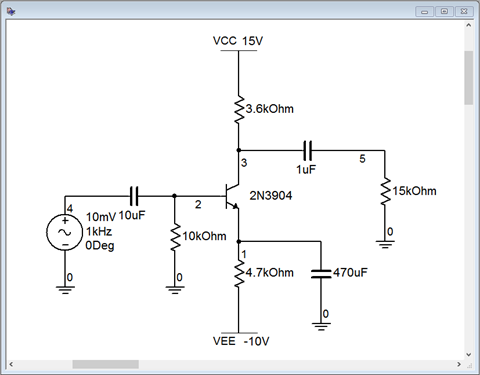
Figure \(\PageIndex{6}\): Unswamped CE amplifier in simulator.
A quick “back-of-an-envelope” estimate gives \(I_C \approx 2\) mA, yielding \(r'_e \approx 13 \Omega \). The load will be around 3 k\( \Omega \) which gives a gain in the low 200s. Thus, we expect the load voltage to be around 2 volts.
The transient analysis graph is depicted in Figure \(\PageIndex{7}\). Several traces are shown.
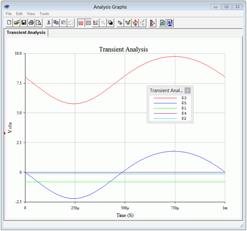
Figure \(\PageIndex{7}\): Unswamped CE amplifier, Transient Analysis.
At this scale, the AC signal at the input (node 4, purple) and the base (node 2, aqua) cannot be seen. As expected, we see a small negative DC value at the base and at the emitter, around −0.7 VDC. The DC offset at the collector is around 8 volts, as expected. Finally, the load voltage (node 5, blue) is sitting right around 2 volts.
What might not be visible immediately in the load voltage plot is some waveform asymmetry distortion. This can be quantified through a THD simulation, the output of which is shown in Figure \(\PageIndex{8}\). THD is nearly 8%. Not so good.
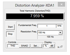
Figure \(\PageIndex{8}\): Non-swamped CE amplifier, THD Analysis.
For the second pass, the circuit is modified to include a swamping resistor, as illustrated in Figure \(\PageIndex{9}\). The original 4.7 k\( \Omega \) emitter resistor has been split into a 4.5 k\( \Omega \) and a 200 \( \Omega \) swamping resistor. The bias in this circuit is identical to the first, therefore \(r'_e\) is unchanged. This will lower our expected gain to around 13, decreasing by a factor of 15. The input signal is raised by a factor of 15 to compensate so that our load voltage will still be around 2 volts.
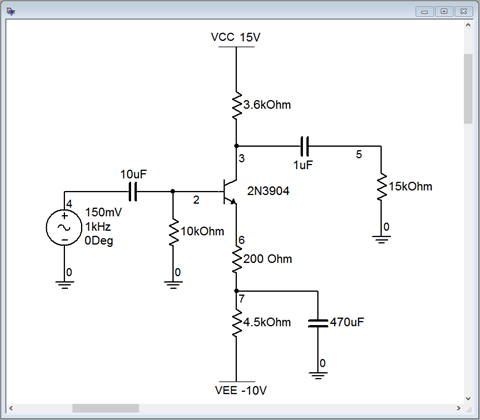
Figure \(\PageIndex{9}\): Swamped CE amplifier in simulator
Once again, we run a transient analysis. The results are shown in Figure \(\PageIndex{10}\). In this case we have done something a little different. By zooming in, we can now confirm the signal inversion. The input signal is the purple trace at node 4. We can also see this signal at the base, riding on the small negative DC bias voltage (aqua trace, node 2). The DC offset is about −0.1 volts. Looking at the emitter we see the expected 0.7 volt DC base-emitter drop below this, or about −0.8 volts DC. Notice that there is no AC signal at the emitter whatsoever. This is expected as the emitter bypass capacitor forces this point to an AC ground.
The load voltage is the blue trace, node 5. While much of it is not visible at this zoom level, clearly it is an inverted waveform when compared to the input signal.
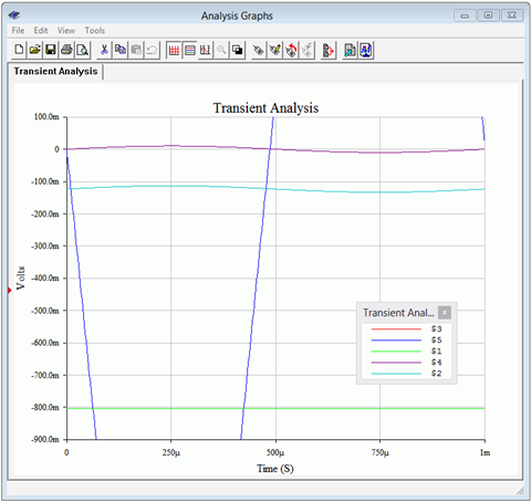
Figure \(\PageIndex{10}\): Swamped CE amplifier, Transient Analysis.
But what about the load voltage distortion? A THD simulation is performed on the swamped amplifier with the results shown in Figure \(\PageIndex{11}\). The THD is now under .6 %, a considerable improvement, even if not audiophile quality. Interestingly, as a ratio, the reduction in distortion is roughly equal to the reduction in gain. The more you give up, the more you get.
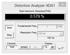
Figure \(\PageIndex{11}\): Swamped CE amplifier, THD Analysis.
Finally, the change in signal quality can be seen readily by plotting both load voltages concurrently, as shown in Figure \(\PageIndex{12}\). The non-swamped output (in blue) exhibits telltale asymmetry. Notice that the positive peak does not quite reach 2 volts but the negative peak exceeds −2 volts. The positive peak is also broadened and flattened, while the negative peak is sharper. In contrast, the swamped output (in red) has virtually identical positive and negative peak values with no apparent shape changes on them. Compare this simulation to the waveform distortion discussion from Chapter 6. In particular, compare Figure \(\PageIndex{12}\) to Figure 6.3.4.
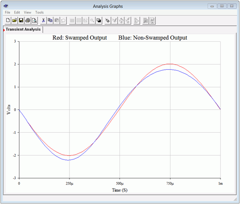
Figure \(\PageIndex{12}\): Swamped versus non-swamped CE amplifiers, Transient Analysis.
7.3.4: Power Supply Bypass and Decoupling
In the prior analyses we have assumed ideal behavior from the DC power sources. First, we assumed that they present a perfect AC ground and second, that they exhibit no ripple or noise. In reality, this may not be the case and non-ideal behavior may lead to a number of problems that diminish the quality of the amplified output signal, including hum and oscillations.
To battle the first issue, power supply bypass capacitors may be used. These capacitors are usually modest in size, perhaps 1 \(\mu\)F or so, although they can be much larger, particularly with high output power amplifiers. Power supply bypass capacitors are located physically close to the active devices. This location minimizes the resistive and inductive effects of power supply circuit board traces and wiring that could result in the power supply not being a good AC ground.
The second issue involves the noise and ripple from the power supply finding its way into the input signal and becoming part of the output signal. A classic example of this is amplifiers that use voltage divider biasing such as the one shown in Figure \(\PageIndex{5}\). Not only does the divider create the needed DC potential at the base terminal, but it also couples in any noise or ripple that might be riding on the DC voltage. This is particularly nasty because this undesirable signal is being applied to the base where it will get amplified.
The obvious solution to this problem is to create a very high quality, regulated DC supply, but this is not always practical given cost constraints. A relatively simple solution is to decouple the undesirable AC components through an \(RC\) network as shown in Figure \(\PageIndex{13}\).
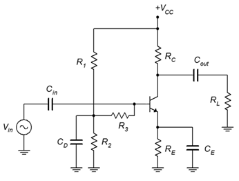
Figure \(\PageIndex{13}\): Decoupled voltage divider.
The capacitor \(C_D\) is used to create an AC ground at the divider junction, thus shunting any noise or ripple to ground. Unfortunately, this would also short out the input signal so \(R_3\) is added to prevent this. \(R_3\) is in parallel with \(Z_{in(base)}\) to create the input impedance.
References
1The obvious question is, “How do we get both high gain and low distortion?” One answer is to use multiple low gain stages in cascade.
2Is “funsies” a real word? It is if we all agree that it is. Besides, if it was an imaginary word, we'd spell it “\(j\) funsies”.