
7.6: Multi-Stage Amplifiers
- Page ID
- 25429

In order to achieve a higher gain than we can obtain from a single stage, it is possible to cascade two or more stages. Different biasing types might be used along with a mix of AC configurations such as a common collector follower for the first stage that drives a common emitter voltage amplifier. A mix of NPN and PNP devices may also be present.
In general terms, each stage serves as the load for the preceding stage. That is, the \(Z_{in}\) of one stage is the \(R_L\) of the previous stage. The gains of the individual stages are then multiplied together to arrive at the system gain. The system input impedance is the input impedance of the first stage only. The source drives the first stage alone. The first stage, in turn, drives the second stage, and so on. Therefore the source only “sees” the first stage because it is the only stage to which it delivers current. In a similar fashion, the output impedance of the system is the \(Z_{out}\) of the last stage. An example is shown in Figure \(\PageIndex{1}\).
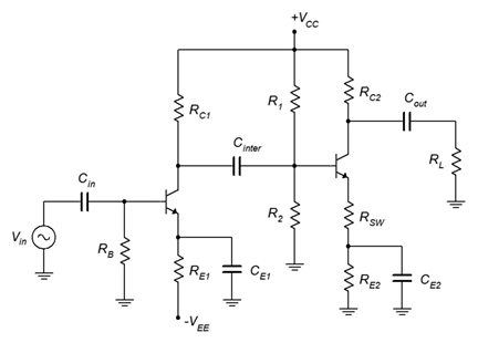
Figure \(\PageIndex{1}\): Two stage amplifier.
In this circuit, stage one is a non-swamped common emitter amplifier utilizing twosupply emitter bias. Stage two is a swamped common emitter amplifier using voltage divider bias. As far as the DC analysis is concerned, these are two separate circuits. The inter-stage coupling capacitor, \(C_{inter}\), prevents the DC potential at the collector of the first transistor from interfering with the bias established by \(R_1\) and \(R_2\) for transistor number two. For the AC computation, the first stage is analyzed in normal fashion except that its load resistance is comprised of \(R_1 || R_2 || Z_{in-base2}\) (i.e., \(Z_{in}\) of stage 2). The second stage is analyzed without changes and its gain is multiplied by the first stage's gain to arrive at the final gain for the pair. The input impedance of the system is \(R_B || Z_{in-base1}\) (i.e., \(Z_{in}\) of stage 1).
It should be obvious that by cascading several stages it is possible to achieve very high system gains, even if each stage is heavily swamped in order to reduce distortion. For example, three swamped common emitter stages with voltage gains of just 10 each would produce a system voltage gain of 1000.
7.6.1: Direct Coupling
With a little creativity, it is possible to create multi-stage designs that use fewer components but which achieve higher performance. One technique is to employ direct coupling of the stages. Direct coupling allows DC to flow from stage to stage. As such, it is possible to design an amplifier that has no lower frequency limit. An example is shown in Figure \(\PageIndex{2}\).
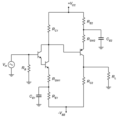
Figure \(\PageIndex{2}\): Direct coupled amplifier.
This two-stage amplifier uses no coupling capacitors nor does it rely on voltage divider resistors for the second stage1. Here is how it works: The first stage is a fairly ordinary swamped common emitter amplifier using two-supply emitter bias. It also uses a Darlington pair to maximize the input impedance. Because the base current is so low, the DC drop on \(R_B\) could be small enough to ignore so we may dispense with the input coupling capacitor. The DC potential at the collector of the Darlington is applied directly to the base of the second stage. This is used to set up the bias of the second stage via the stage two emitter resistors. This is precisely what we did with the circuit of Figure 7.3.5. The only difference is that here the base voltage is derived from the preceding stage instead of from a voltage divider. The computations for \(I_C\), \(r'_e\) and the like would proceed unchanged. In any event, this eliminates two biasing resistors and another coupling capacitor.
Note the use of the PNP device for the second stage. By using a PNP, its collector voltage must be less than its emitter voltage. As we're also using a bipolar power supply, we can eliminate the need for the final output coupling capacitor. All we need to do is set up the resistor values such that the drop across \(R_{C2}\) is the same as \(V_{EE}\). This will place the stage two DC collector voltage at 0 volts. If there's no DC voltage then there's nothing to block, and therefore no need for the coupling capacitor.
References
1This circuit does use emitter bypass capacitors so the DC gain will be less than the AC gain. In that sense we might say that this amplifier is not fully DC coupled.