
8.5: Power Transistor Data Sheet Interpretation
- Page ID
- 25435

The data sheet for a popular NPN power transistor, the 2N3055, is shown in Figure \(\PageIndex{1}\). This model is available from several different manufacturers. Due to the high power dissipation, the TO-92 plastic case that is used for small signal devices is not appropriate. Instead, this device uses the all-metal TO-3 case. Under the maximum ratings we find the device has a maximum power dissipation of 115 W at a case temperature of 25\(^{\circ}\) C, a maximum collector current of 15 A and a maximum collector-emitter voltage of 60 V. Obviously, the device cannot withstand maximum current and voltage simultaneously.
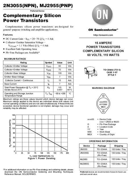
Figure \(\PageIndex{1a}\): 2N3055 data sheet. Used with permission from SCILLC dba ON Semiconductor.
In the drawing of the TO-3 case, only two leads are shown. These are for the emitter and base. The entire body of the device is the collector. This is because the device will most likely be attached to a metal heat sink (see next section) to help dissipate the heat generated. The greater the contact area, the more effective the heat flow will be. The curves presented in Figure \(\PageIndex{1b}\) indicate that \(\beta\) is considerably lower than what we saw for small signal devices. Further, \(I_{C(sat)}\) tends to be larger for higher power transistors. For very high currents, \(\beta\) might fall to less than 20 while \(I_{C(sat)}\) can be upwards of half of a volt.
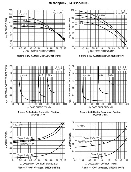
Figure \(\PageIndex{1b}\): 2N3055 data sheet (cont).
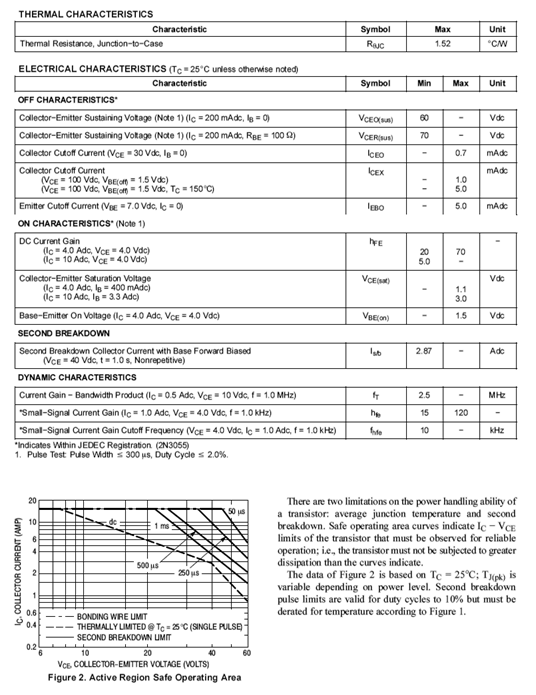
Figure \(\PageIndex{1c}\): 2N3055 data sheet (cont).
One item of note in Figure \(\PageIndex{1c}\) is the small graphic at the bottom of the sheet. This is a plot of safe operating area. Basically, the combination of \(V_{CE}\) and \(I_C\) must fall within the lower-left zone. What is of particular interest is that the safe zone extends out further if the current/voltage combination is the result of a short pulse rather than a continuous condition.
8.5.1: Power Derating
One final item of concern is the graph found in Figure \(\PageIndex{1a}\), and magnified in Figure \(\PageIndex{2}\). This is a power derating curve.
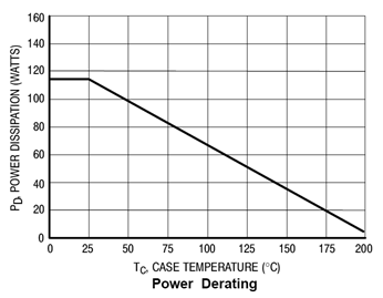
Figure \(\PageIndex{2}\): Power derating curve for 2N3055. Used with permission from SCILLC dba ON Semiconductor.
Although the device is rated for 115 watts, that is only true at case temperatures of 25\(^{\circ}\)C or lower. At higher temperatures, the power dissipation capability decreases. For example, at 100\(^{\circ}\)C this device can only dissipate about 65 watts. A precise value can be computed via the following formula:
\[P_D = P_{25} − D(T_{case} − 25^{\circ}C) \label{8.8} \]
Where
\(P_D\) is the power dissipation at the new case temperature,
\(P_{25}\) is the power dissipation at 25\(^{\circ}\)C,
\(D\) is the derating factor (units of W/C\(^{\circ}\)),
\(T_{case}\) is the new case temperature.
Example \(\PageIndex{1}\)
Determine the power dissipation of a 2N3055 at 75\(^{\circ}\)C.
Using the graph, this is a little over 80 watts.
For a more accurate result, we'll use Equation \ref{8.8}. From the data sheet the dissipation at 25\(^{\circ}\)C, \(P_{25}\), is 115 watts. The derating factor, \(D\), is 0.657 W/C\(^{\circ}\) (the derating factor is found directly above the graph of power derating in Figure \(\PageIndex{1a}\)).
\[P_D = P_{25}−D(T_{ambient}−25^{\circ}C) \nonumber \]
\[P_D = 115W −0.657W/C^{\circ}(75^{\circ}C−25^{\circ}C) \nonumber \]
\[P_D = 82.1W \nonumber \]