
12.3: DE-MOSFET Biasing
- Page ID
- 25328

As the characteristic equations of the JFET and DE-MOSFET are the same, the DC biasing model is the same. Consequently, the DE-MOSFET can be biased using any of the techniques used with the JFET including self bias, combination bias and current source bias as these are all second quadrant biasing schemes (i.e., have a negative \(V_{GS}\)). The self bias and combination bias equations and plots from Chapter 10 may be used without modification. The DE-MOSFET also allows first quadrant operation so a couple of new biasing forms become available: zero bias and voltage divider bias. In reality, both are variations on constant voltage bias but which utilize the first quadrant.
12.3.1: Zero Bias
Zero bias is unique. In some ways it can be thought of as a cross between self bias and constant voltage bias. Like self bias, it does not require a second DC source for the gate or source terminal. Like constant voltage bias, there is no need for a source resistor, \(R_S\). A prototype of zero bias is shown in Figure \(\PageIndex{1}\). There is no question that it is a minimal parts-count circuit.
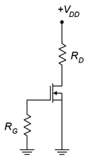
Figure \(\PageIndex{1}\): Zero bias prototype.
Zero bias is so named because it operates at \(V_{GS} = 0\) V. Recall that the gate current is ideally zero, thus there is no drop across \(R_G\) and \(V_G = 0\) V as a consequence. The source is tied directly to ground, therefore \(V_{GS}\) must equal 0 V. As \(V_{GS}\) doesn't change, this can be thought of as a form of constant voltage bias. The interesting bit is that when an AC signal is applied to the gate, its negative portion will pull the MOSFET down into depletion mode and the positive portion will push the operation into enhancement mode. Because the device can operate in this fashion, conducting current while straddling zero, so to speak, DE-MOSFETs are sometimes referred to as normally on devices.
Determining the operating point for zero bias is startlingly easy. Because \(V_{GS} = 0\) V, \(I_D\) must equal \(I_{DSS}\) and \(g_m\) must equal \(g_{m0}\). Like all constant voltage biasing schemes, though, Q point stability is not very good. Another point to notice is that, as there is no source resistor, this bias is only applicable to non-swamped common source amplifiers. It cannot be used with a source follower or swamped amplifier (if a small swamping resistor is inserted into the source, technically the circuit can be classified as self bias, although the AC signal may still push operation into enhancement mode).
Example \(\PageIndex{1}\)
Determine \(I_D\), \(V_D\) and \(g_{m0}\) for the circuit shown in Figure \(\PageIndex{2}\). Assume \(I_{DSS} = 12\) mA and \(V_{GS(off)} = −3\) V.
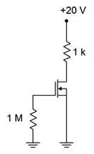
Figure \(\PageIndex{2}\): Circuit for Example \(\PageIndex{1}\).
By inspection, as this is zero bias \(I_D = I_{DSS}\), and therefore \(I_D = 12\) mA. Using KVL and Ohm's law we can find \(V_D\).
\[V_D = V_{DD} −I_D R_D \nonumber \]
\[V_D = 20 V−12 mA \times 1k \Omega \nonumber \]
\[V_D = 8 V \nonumber \]
\[g_{m0} =− \frac{2 I_{DSS}}{V_{GS (off )}} \nonumber \]
\[g_{m0} =− \frac{2 \times 12mA}{−3V} \nonumber \]
\[g_{m0} = 8mS \nonumber \]
12.3.2: Voltage Divider Bias
Voltage divider bias is a form of constant voltage bias that operates in enhancement mode. A prototype circuit is shown in Figure \(\PageIndex{3}\). Note that the source terminal is connected directly to ground. This is important. If this was not the case, this would be a form of combination bias (basically shifting the \(V_{SS}\) supply up to ground and then shifting the gate voltage from ground up to a positive \(V_{SS}\) to maintain the same differential voltage). As such, it would be operating in depletion mode.
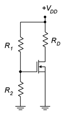
Figure \(\PageIndex{3}\): Voltage divider bias prototype.
The voltage divider comprised of \(R_1\) and \(R_2\) will establish a DC bias potential on the gate. As the source is at ground, \(V_{GS} = V_G = V_{R2}\). Given that \(V_{DD}\) must be positive, then \(V_{GS}\) must be positive, and enhancement mode operation is a given.
The most direct way to handle this is to determine the voltage divider potential and use either the characteristic equation (Equation 10.2.1) or associated graph to determine the drain current. Once \(I_D\) is found, the drain-source voltage may be found via the standard Ohm's law/KVL route.
Before continuing, note that the values of the divider resistors can be very high without creating biasing problems (unlike the BJT version of voltage divider bias). This is because the gate current is so small that even when using megohm values for the divider, the loading caused by the gate will not be noticeable.
Example \(\PageIndex{2}\)
For the circuit of Figure \(\PageIndex{4}\), determine \(I_D\) and \(V_D\). Assume \(I_{DSS} = 2\) mA and \(V_{GS(off)} = −6\) V.
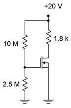
Figure \(\PageIndex{4}\): Circuit for Example \(\PageIndex{2}\).
The voltage divider will yield \(V_{GS}\).
\[V_{GS} = V_{DD} \left( \frac{R_2}{R_1+R_2} \right) \nonumber \]
\[V_{GS} = 20 V \left( \frac{2.5M \Omega}{ 10 M \Omega +2.5M \Omega} \right) \nonumber \]
\[V_{GS} = 4 V \nonumber \]
Use Equation 10.2.1 to find \(I_D\).
\[I_D = I_{DSS} \left( 1 − \frac{V_{GS}}{V_{GS (off )}} \right)^2 \nonumber \]
\[I_D = 2 mA \left( 1 − \frac{4V}{−6V} \right)^2 \nonumber \]
\[I_D = 5.56 mA \nonumber \]
Use KVL and Ohm's law to find \(V_D\).
\[V_D = V_{DD} −I_D R_D \nonumber \]
\[V_D = 20 V−5.56 mA \times 1.8k \Omega \nonumber \]
\[V_D = 9.99 V \nonumber \]
Alternately, using the curve of Figure 12.2.3, we would first find the normalized gate-source voltage which is 4 V/6 V or 0.667 (note that the curve plots \(−V_{GS}/V_{GS(off)}\) so that the quadrants do not appear reversed). From this the normalized drain current, \(I_D/I_{DSS}\), may be determined to be approximately 2.8, yielding a drain current of 5.6 mA.