
12.6: E-MOSFET Biasing
- Page ID
- 25331

As the E-MOSFET operates only in the first quadrant, none of the biasing schemes used with JFETs will work with it. First, it should be noted that for large signal switching applications biasing is not much of an issue as we simply need to confirm that there is sufficient drive signal to turn the device on. For linear amplifiers we can use variations on constant voltage bias such as voltage divider bias, or on drain feedback bias.
12.6.1: Voltage Divider Bias
Voltage divider bias is reminiscent of the divider circuit used with BJTs. Indeed, the N-channel E-MOSFET requires that its gate be higher than its source, just as the NPN BJT requires a base voltage higher than its emitter. The major differences between the two are that the E-MOSFET's input gate current is negligible compared to base current and that the gate-source voltage will be most likely higher than the 0.7 volt drop seen across the base-emitter junction. Also, the gate-source voltage will not be locked to a specific voltage but will vary depending on the remainder of the circuit.
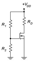
Figure \(\PageIndex{1}\): Voltage divider bias for E-MOSFET.
The prototype for the voltage divider bias is shown in Figure \(\PageIndex{1}\). In general, the layout it is the same as the voltage divider bias used with the DE-MOSFET. The resistors \(R_1\) and \(R_2\) set up the divider to establish the gate voltage. As the source terminal is tied directly to ground, this means that \(V_{GS} = V_G\). The potential across \(R_2\) needs to be set above \(V_{GS(th)}\) for proper operation in accordance with Equation 12.4.1. Knowing the value of \(V_G\), either the characteristic equation or the corresponding normalized drain current plot can be used to determine the drain current. The only factor missing is the device constant, \(k\). This can be computed for any particular device based on the \(I_{D(on)}\), \(V_{GS(on)}\) coordinate pair specified in the data sheet (or measured in lab). An example is shown in Figure \(\PageIndex{2}\).
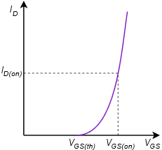
Figure \(\PageIndex{2}\): Coordinate pair on E-MOSFET curve.
The constant \(k\) is found via a rearrangement of Equation 12.4.1:
\[k = \frac{I_{D(on )}}{(V_{GS (on )} −V_{GS (th )} )^2} \nonumber \]
This value can then be used for other biasing points.
Example \(\PageIndex{1}\)
For the circuit and matching device curve of Figure \(\PageIndex{3}\), find \(I_D\) and \(V_{DS}\).
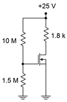
Figure \(\PageIndex{3a}\): Circuit for Example \(\PageIndex{1}\).
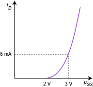
Figure \(\PageIndex{3b}\): Device curve for Example \(\PageIndex{1}\).
First find the value of \(k\):
\[k = \frac{I_{D(on )}}{(V_{GS (on )}−V_{GS (th )} )^2} \nonumber \]
\[k = \frac{6 mA}{(3 V −2 V)^2} \nonumber \]
\[k = 6 mA/V^2 \nonumber \]
Now determine the gate voltage:
\[V_G = V_{DD} \frac{R_2}{R_1+R_2} \nonumber \]
\[V_G = 25 V \frac{1.5M \Omega}{10 M \Omega +1.5M \Omega} \nonumber \]
\[V_G = 3.26 V \nonumber \]
The source is grounded so \(V_{GS} = V_G\).
\[I_D = k (V_{GS} −V_{GS (th)} )^2 \nonumber \]
\[I_D = 6mA/V^2 (3.26 V −2 V)^2 \nonumber \]
\[I_D = 9.54 mA \nonumber \]
\[V_{DS} = V_{DD} −I_D R_D \nonumber \]
\[V_{DS} = 25V−9.54 mA \times 1.8 k \Omega \nonumber \]
\[V_{DS} = 7.83 V \nonumber \]
In closing, note that it is possible to decouple the voltage divider using the same method employed with BJTs in Figure 7.3.11. Very large value resistors are available in only a limited variety of sizes so this technique has an added benefit. The divider resistors can use more convenient sizes because \(R_1\) and \(R_2\) will not set the input impedance; it will be set by the decoupling resistor.
12.6.2: Drain Feedback Bias
Drain feedback bias utilizes the aforementioned “on” operating point from the characteristic curve. The idea is to establish a drain current via an appropriate selection of the drain resistor and power supply. The prototype of the drain feedback circuit is shown in Figure \(\PageIndex{4}\).
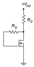
Figure \(\PageIndex{4}\): Drain feedback bias prototype.
This is relatively simple layout using few components. The key to understanding its operation is the KVL summation:
\[V_{DD} = V_{R_{D}} +V_{R_G} +V_{GS} \nonumber \]
\[V_{DD} = I_D R_D+I_G R_G+V_{GS} \nonumber \]
Gate current is negligible which means that
\[V_{DD} = I_D R_D+V_{GS} \nonumber \]
and also
\[V_{DS} = V_{GS} \nonumber \]
Therefore,
\[V_{GS} = V_{DS} = V_{DD} −I_D R_D \label{12.7} \]
Equation \ref{12.7} can be used as the basis for the design of the bias circuit.
Example \(\PageIndex{2}\)
Utilizing the prototype of Figure \(\PageIndex{4}\), determine values for \(R_D\) and \(R_G\) such that the drain current is 8 mA. Assume \(V_{DD} = 20\) V, \(I_{D(on)} = 5\) mA at \(V_{GS(on) = 4}\) V, and \(V_{GS(th)} = 2.5\) V.
First find the value of \(k\):
\[k = \frac{I_{D(on)}}{(V_{GS (on)} − V_{GS (th)} )^2} \nonumber \]
\[k = \frac{5mA}{(4 V −2.5 V)^2} \nonumber \]
\[k = 2.22mA/V^2 \nonumber \]
Now determine the required \(V_{GS}\) to obtain 8 mA of drain current by rearranging Equation 12.4.1.
\[I_D = k(V_{GS} −V_{GS (th)} )^2 \nonumber \]
\[V_{GS} = V_{GS (th)} + \sqrt{\frac{I_D}{k}} \nonumber \]
\[V_{GS} = 2.5V+ \sqrt{\frac{8mA}{2.22 mA/V^2}} \nonumber \]
\[V_{GS} = 4.4 V \nonumber \]
And finally,
\[V_{GS} = V_{DS} = V_{DD} −I_D R_D \nonumber \]
\[R_D = \frac{V_{DD} − V_{GS}}{I_D} \nonumber \]
\[R_D = \frac{20 V −4.4 V}{8mA} \nonumber \]
\[R_D = 1.95 k \Omega \nonumber \]