
13.2: MOSFET Common Source Amplifiers
- Page ID
- 25334

Before we can examine the common source amplifier, an AC model is needed for both the DE- and E-MOSFET. A simplified model consists of a voltage-controlled current source and an input resistance, \(r_{GS}\). This model is shown in Figure \(\PageIndex{1}\). The model is essentially the same as that used for the JFET. Technically, the gate-source resistance is higher in the MOSFET due to the insulated gate, and this is useful in specific applications such as in the design of electrometers, but for general purpose work it is a minor distinction. The impedance associated with the current source is not shown as it is typically large enough to ignore. Similarly, the device capacitances are not shown. It is worth noting that the capacitances associated with small signal devices might be just a few picofarads, however, a power device might exhibit values of a few nanofarads.
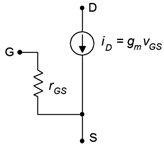
Figure \(\PageIndex{1}\): AC device model for MOSFETs.
As the device model is the same for both DE- and E-MOSFETs, the analysis of voltage gain, input impedance and output impedance will apply to both devices. The only practical differences will be how the transconductance is determined, and circuit variations due to the differing biasing requirements which will effect the input impedance. In fact, there will be a great uniformity between JFET-based circuits and DE-MOSFET circuits operating in depletion mode.
An AC equivalent of a swamped common source amplifier is shown in Figure \(\PageIndex{2}\). This is a generic prototype and is suitable for any variation on device and bias type. Ultimately, all of the amplifiers can be reduced down to this equivalent, occasionally with some resistance values left out (either opened or shorted). For example, if the amplifier is not swamped then \(r_S = 0\). Similarly, \(r_G\) might correspond to a single gate biasing resistor or it might represent the equivalent of a pair of resistors that set up a gate voltage divider.
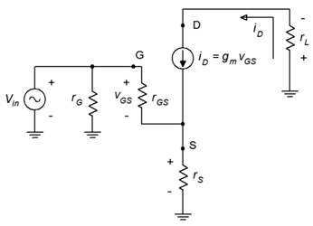
Figure \(\PageIndex{2}\): Generic common source amplifier equivalent.
13.2.1: Voltage Gain
In order to derive an equation for the voltage gain, we start with its definition, namely that voltage gain is the ratio of \(v_{out}\) to \(v_{in}\). We then proceed by expressing these voltages in terms of their Ohm's law equivalents. Note that \(r_L\) can also be called \(r_D\).
\[A_v = \frac{v_{out}}{v_{i n}} = \frac{v_L}{v_G} = \frac{v_D}{v_G} \\ A_v = \frac{−i_D r_L}{i_D r_S+v_{GS}} \\ A_v = \frac{−g_m v_{GS} r_L}{g_m v_{GS} r_S+v_{GS}} \\ A_v =− \frac{g_m r_L}{g_m r_S+1} \label{13.1} \]
or, if preferred
\[A_v =− \frac{g_m r_D}{g_m r_S+1} \label{13.1b} \]
This is the general equation for voltage gain. If the amplifier is not swamped then the first portion of the denominator drops out and the gain simplifies to
\[A_v = −g_m r_L \label{13.2} \]
or alternately
\[A_v = −g_m r_D \label{13.2b} \]
The swamping resistor, \(r_S\), plays the same role here as it did with both the BJT and JFET. Swamping helps to stabilize the gain and reduce distortion, but at the expense of voltage gain.
13.2.2: Input Impedance
Referring back to Figure \(\PageIndex{2}\), the input impedance of the amplifier will be \(r_G\) in parallel with the impedance looking into the gate terminal, \(Z_{in(gate)}\). At a minimum this will be \(r_{GS}\) (it is somewhat higher when swamped but this can be ignored in most cases). At low frequencies \(r_{GS}\) is very large, perhaps as high as \(10^{12}\) ohms. In most practical circuits, \(r_G\) will be much lower, hence
\[Z_{in} = r_G || r_{GS} \approx r_G \label{13.3} \]
It is important to reiterate that \(r_G\) is the equivalent resistance seen prior to the gate terminal that is seen from the vantage point of \(V_{in}\). In the case of self bias, combination bias, zero bias and constant current bias, this will be the single biasing resistor \(R_G\). For simple voltage divider biasing, \(r_G\) will be the parallel combination of the two divider resistors (i.e., \(R_1 || R_2\)). For decoupled voltage divider biasing, as shown in Figure \(\PageIndex{3}\), \(r_G\) will be the decoupling resistor (i.e., \(R_3\)) that is connected between the divider and the gate. This is because the divider node is bypassed to ground via a capacitor. Finally, for drain feedback biasing, \(r_G\) is the Millerized \(R_G\) that bridges the drain and gate.
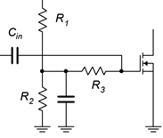
Figure \(\PageIndex{3}\): Decoupled voltage divider.
13.2.3: Output Impedance
The derivation of output impedance is unchanged from the JFET case. From the perspective of the load, the output impedance will be the drain biasing resistor, \(R_D\), in parallel with the internal impedance of the current source within the device model. \(R_D\) tends to be much lower than this, and thus, the output impedance can be approximated as \(R_D\).
Therefore we may state
\[Z_{out} = r_{model} || R_D \approx R_D \label{13.4} \]
At this point, a variety of examples are in order to illustrate some of the myriad combinations.
Example \(\PageIndex{1}\)
For the amplifier in Figure \(\PageIndex{4}\), determine the input impedance and load voltage. \(V_{in}\) = 20 mV, \(V_{DD}\) = 20 V, \(R_G\) = 1 M\(\Omega\), \(R_D\) = 1.8 k\(\Omega\), \(R_{SW}\) = 20 \(\Omega\), \(R_S\) = 400 \(\Omega\), \(R_L\) = 12 k\(\Omega\), \(I_{DSS}\) = 40 mA, \(V_{GS(off)}\) = −1 V.
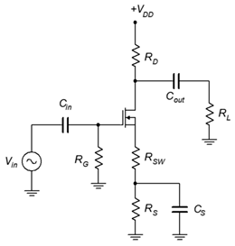
Figure \(\PageIndex{4}\): Circuit for Example \(\PageIndex{1}\).
This is a swamped common drain amplifier utilizing self bias. \(Z_{in}\) can be determined via inspection.
\[Z_{i n} = Z_{i n(gate)} || R_G \nonumber \]
\[Z_{i n} \approx 1 M\Omega \nonumber \]
To find the load voltage we'll need the voltage gain, and to find the gain we'll first need to find \(g_{m0}\).
\[g_{m0} =− \frac{2 I_{DSS}}{V_{GS (off )}} \nonumber \]
\[g_{m0} =− \frac{80 mA}{−1V} \nonumber \]
\[g_{m0} = 80mS \nonumber \]
The combined DC value of \(R_S\) is 420 \(\Omega\), therefore \(g_{m0}R_S\) = 33.6. From the self bias equation or graph this produces a drain current of 1.867 mA.
\[g_m = g_{m0} \sqrt{\frac{I_D}{I_{DSS}}} \nonumber \]
\[g_m = 80 mS \sqrt{\frac{1.867 mA}{40mA}} \nonumber \]
\[g_m = 17.3mS \nonumber \]
The swamping resistor, \(r_S\), is 20 \(\Omega\). The voltage gain is
\[A_v = − \frac{g_m r_L}{g_m r_S+1} \nonumber \]
\[A_v =− \frac{17.3 mS(1.8k\Omega || 12 k \Omega )}{17.3mS \times 20\Omega +1} \nonumber \]
\[A_v =−20.1 \nonumber \]
And finally
\[V_{load} = A_v V_{i n} \nonumber \]
\[V_{load} =−20.1 \times 20mV \nonumber \]
\[V_{load} = 402mV \nonumber \]
Computer Simulation
The amplifier of Example \(\PageIndex{1}\) is simulated to verify the results. The circuit is entered into the simulator as shown in Figure \(\PageIndex{5}\). One issue is finding an appropriate DE-MOS device to match the parameters used in the example. The BSS229 proves to be reasonably close. This device model was tested for \(I_{DSS}\) by applying a 20 volt source to the drain and shorting the source and gate terminals to ground in the simulator. The current was just under the 40 mA target. Similarly, a negative voltage was attached to the gate and adjusted until the drain current dropped to nearly zero in order to determine \(V_{GS(off)}\). The model's value was just under the desired −1 volt. Consequently, we can expect the simulation results to be close to those predicted, although not identical.
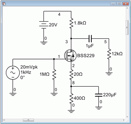
Figure \(\PageIndex{5}\): The circuit of Example \(\PageIndex{1}\) in the simulator.
The transient analysis is run next and is shown in Figure \(\PageIndex{6}\). The expected signal inversion is obvious. The peak amplitude is 417 mV, just a few percent higher than the calculated value. At least some of this deviation is due to the model's variation from the assumed device parameter values.
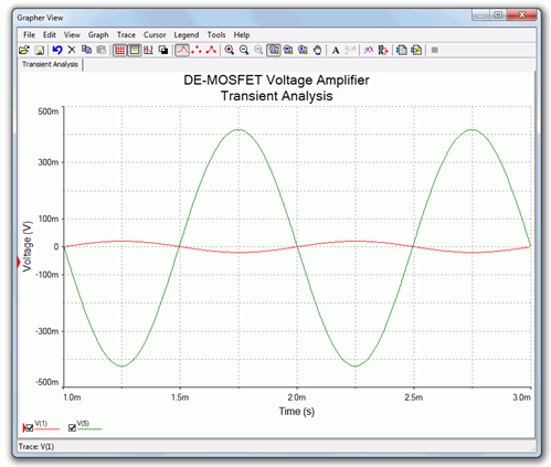
Figure \(\PageIndex{6}\): Transient analysis simulation for the circuit of Example \(\PageIndex{1}\).
A DC bias check is also performed. The drain current was calculated to be 1.867 mA. This yields an \(R_D\) voltage of a little over 3 volts, thus we expect to see a drain voltage of about 17 volts. Similarly, we would expect the source terminal to be sitting at around 700 to 800 mV and the gate at about 0 V.
The results of the DC operating point simulation are shown in Figure \(\PageIndex{7}\). The agreement with the predicted values is quite good, especially considering that the device model is not a perfect match.
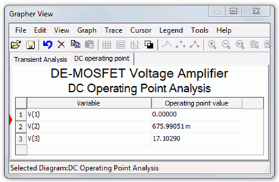
Figure \(\PageIndex{7}\): DC bias simulation for the circuit of Example \(\PageIndex{1}\).
Example \(\PageIndex{2}\)
For the circuit of Figure \(\PageIndex{8}\), determine the voltage gain and input impedance. Assume \(V_{GS(th)}\) = 2 V, \(I_{D(on)}\) = 50 mA at \(V_{GS(on)}\) = 5 V.
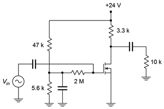
Figure \(\PageIndex{8}\): Circuit for Example \(\PageIndex{2}\).
First find the value of \(k\):
\[k = \frac{I_{D(on )}}{(V_{GS (on )} − V_{GS (th )} )^2} \nonumber \]
\[k = \frac{50mA}{(5V −2 V)^2} \nonumber \]
\[k = 5.56 mA/V^2 \nonumber \]
This circuit uses power supply decoupling. The voltage drop across the 2 M\(\Omega\) resistor is small enough to ignore as the current passing through it is gate current. Therefore the gate voltage is determined by the divider. Also, as the left end of the 2 M\(\Omega\) resistor is tied to an AC ground due to the bypass capacitor, it represents the input impedance.
\[Z_{in} = 2 M\Omega || Z_{in(gate)} \approx 2 M\Omega \nonumber \]
\[V_G = V_{DD} \frac{R_2}{R_1+R_2} \nonumber \]
\[V_G = 24 V \frac{5.6 k\Omega}{47k \Omega +5.6 k\Omega} \nonumber \]
\[V_G = 2.56 V \nonumber \]
The source is grounded so \(V_{GS} = V_G\).
\[I_D = k (V_{GS} −V_{GS (th)} )^2 \nonumber \]
\[I_D = 5.56 mA/V^2 (2.56 V −2V)^2 \nonumber \]
\[I_D = 1.74 mA \nonumber \]
\[g_m = 2 k (V_{GS} −V_{GS (th)} ) \nonumber \]
\[g_m = 2 \times 5.56 mA/V^2 (2.56 V −2V) \nonumber \]
\[g_m = 6.23 mS \nonumber \]
This amplifier is not swamped so the simplified gain equation may be used.
\[A_v =−g_m r_D \nonumber \]
\[A_v =−6.23mS(3.3 k\Omega || 10 k \Omega ) \nonumber \]
\[A_v =−15.5 \nonumber \]
Example \(\PageIndex{3}\)
For the circuit of Figure \(\PageIndex{9}\), determine the voltage gain and input impedance. Assume \(V_{GS(off)}\) = −0.75 V and \(I_{DSS}\) = 6 mA.
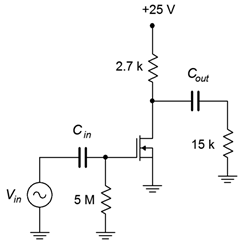
Figure \(\PageIndex{9}\): Circuit for Example \(\PageIndex{3}\).
This amplifier uses zero bias, therefore \(I_D = I_{DSS}\) and \(g_m = g_{m0}\).
\[g_{m0} =− \frac{2 I_{DSS}}{V_{GS (off )}} \nonumber \]
\[g_{m0} =− \frac{2 \times 6 mA}{−0.75 V} \nonumber \]
\[g_{m0} = 16mS \nonumber \]
This amplifier is not swamped so we may use the simplified equation for voltage gain.
\[A_v =−g_m r_D \nonumber \]
\[A_v =−16mS(2.7k \Omega || 15k \Omega ) \nonumber \]
\[A_v =−36.6 \nonumber \]
Finally, for the input impedance we have
\[Z_{in} = 5 M\Omega || Z_{in(gate)} \approx 5 M\Omega \nonumber \]