
13.5: Exercises
- Page ID
- 25337

13.5.1: Analysis Problems
1. For the amplifier of Figure \(\PageIndex{1}\), determine \(Z_{in}\) and \(A_v\). \(V_{in}\) = 20 mV, \(I_{DSS}\) = 10 mA, \(V_{GS(off)}\) = −2 V, \(V_{DD}\) = 20 V, \(R_G\) = 750 k\(\Omega\), \(R_D\) = 2 k\(\Omega\), \(R_L\) = 4 k\(\Omega\), \(R_S\) = 1 k\(\Omega\), \(R_{SW}\) = 200 \(\Omega\).
2. For the amplifier of Figure \(\PageIndex{1}\), determine \(Z_{in}\) and \(V_{out}\). \(V_{in}\) = 25 mV, \(I_{DSS}\) = 15 mA, \(V_{GS(off)}\) = −2 V, \(V_{DD}\) = 22 V, \(R_G\) = 330 k\(\Omega\), \(R_D\) = 2 k\(\Omega\), \(R_L\) = 6 k\(\Omega\), \(R_S\) = 510 \(\Omega\), \(R_{SW}\) = 220 \(\Omega\).
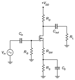
Figure \(\PageIndex{1}\)
3. For the circuit of Figure \(\PageIndex{2}\), determine \(Z_{in}\) and \(A_v\). \(V_{in}\) = 10 mV, \(I_{DSS}\) = 12 mA, \(V_{GS(off)}\) = −2.5 V, \(V_{DD}\) = 26 V, \(R_G\) = 510 k\(\Omega\), \(R_D\) = 1.2 k\(\Omega\), \(R_L\) = 25 k\(\Omega\).
4. For the circuit of Figure \(\PageIndex{2}\), determine \(Z_{in}\) and \(V_{out}\). \(V_{in}\) = 25 mV, \(I_{DSS}\) = 15 mA, \(V_{GS(off)}\) = −1.5 V, \(V_{DD}\) = 24 V, \(R_G\) = 820 k\(\Omega\), \(R_D\) = 1 k\(\Omega\), \(R_L\) = 12 k\(\Omega\).
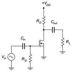
Figure \(\PageIndex{2}\)
5. For the circuit of Figure \(\PageIndex{3}\), determine \(Z_{in}\) and \(V_{out}\). \(V_{in}\) = 25 mV, \(I_{DSS}\) = 8 mA, \(V_{GS(off)}\) = −3.5 V, \(V_{DD}\) = 24 V, \(R_1\) = 1 M\(\Omega\), \(R_2\) = 100 k\(\Omega\), \(R_D\) = 800 \(\Omega\), \(R_L\) = 10 k\(\Omega\).
6. For the circuit of Figure \(\PageIndex{3}\), determine \(Z_{in}\) and \(A_v\). \(V_{in}\) = 10 mV, \(I_{DSS}\) = 6 mA, \(V_{GS(off)}\) = −4 V, \(V_{DD}\) = 26 V, \(R_1\) = 2 M\(\Omega\), \(R_2\) = 120 k\(\Omega\), \(R_D\) = 1.2 k\(\Omega\), \(R_L\) = 15 k\(\Omega\).

Figure \(\PageIndex{3}\)
7. For the circuit of Figure \(\PageIndex{4}\), determine \(Z_{in}\) and \(V_{out}\). \(V_{in}\) = 20 mV, \(I_{D(on)}\) = 6 mA at \(V_{DS(on)}\) = 3 V, \(V_{GS(th)}\) = 2.5 V, \(V_{DD}\) = 34 V, \(R_1\) = 1 M\(\Omega\), \(R_2\) = 100 k\(\Omega\), \(R_D\) = 1 k\(\Omega\), \(R_L\) = 10 k\(\Omega\).
8. For the circuit of Figure \(\PageIndex{4}\), determine \(Z_{in}\) and \(A_v\). \(V_{in}\) = 15 mV, \(I_{D(on)}\) = 10 mA at \(V_{DS(on)}\) = 4 V, \(V_{GS(th)}\) = 2 V, \(V_{DD}\) = 30 V, \(R_1\) = 2 M\(\Omega\), \(R_2\) = 180 k\(\Omega\), \(R_D\) = 1.2 k\(\Omega\), \(R_L\) = 15 k\(\Omega\).
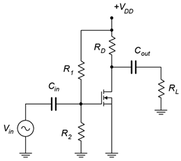
Figure \(\PageIndex{4}\)
9. For the circuit of Figure \(\PageIndex{5}\), determine \(Z_{in}\) and \(V_{out}\). \(V_{in}\) = 200 mV, \(I_{DSS}\) = 15 mA, \(V_{GS(off)}\) = −3 V, \(V_{DD}\) = 15 V, \(R_G\) = 910 k\(\Omega\), \(R_L\) = 10 k\(\Omega\), \(R_S\) = 330 \(\Omega\).
10. For the circuit of Figure \(\PageIndex{5}\), determine \(Z_{in}\) and \(V_{out}\). \(V_{in}\) = 200 mV, \(I_{DSS}\) = 20 mA, \(V_{GS(off)}\) = −2 V, \(V_{DD}\) = 12 V, \(R_G\) = 1 M\(\Omega\), \(R_L\) = 1.8 k\(\Omega\), \(R_S\) = 220 \(\Omega\).
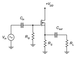
Figure \(\PageIndex{5}\)
11. For the circuit of Figure \(\PageIndex{6}\), determine \(Z_{in}\) and \(A_v\). \(I_{DSS}\) = 18 mA, \(V_{GS(off)}\) = −2 V, \(V_{DD}\) = 12 V, \(V_{SS}\) = −4 V, \(R_G\) = 680 k\(\Omega\), \(R_L\) = 10 k\(\Omega\), \(R_S\) = 1 k\(\Omega\).
12. For the circuit of Figure \(\PageIndex{6}\), determine \(Z_{in}\) and \(A_v\). \(I_{DSS}\) = 20 mA, \(V_{GS(off)}\) = −2 V, \(V_{DD}\) = 10 V, \(V_{SS}\) = −6 V, \(R_G\) = 2.2 M\(\Omega\), \(R_L\) = 5 k\(\Omega\), \(R_S\) = 510 \(\Omega\).
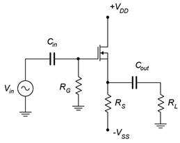
Figure \(\PageIndex{6}\)
13.5.2: Design Problems
13. Following the circuit of Figure \(\PageIndex{1}\), design an amplifier with a gain of at least 5 and an input impedance of at least 500 k\(\Omega\). \(R_L\) = 10 k\(\Omega\). The MOSFET has the following parameters: \(V_{GS(off)}\) = −2 V, \(I_{DSS}\) = 25 mA. Try to use standard resistor values.
14. Using the circuit of Figure \(\PageIndex{5}\), design a follower with a gain of at least .75 and an input impedance of at least 1 M\(\Omega\). \(R_L\) = 2 k\(\Omega\). The MOSFET has the following parameters: \(V_{GS(off)}\) = −1.5 V, \(I_{DSS}\) = 40 mA. Try to use standard resistor values.
13.5.3: Challenge Problems
15. For the circuit of Figure \(\PageIndex{7}\), determine \(Z_{in}\) and \(A_v\). \(I_{DSS}\) = 15 mA, \(V_{GS(off)}\) = −2 V.
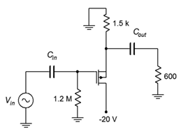
Figure \(\PageIndex{7}\)
16. For the circuit of Figure \(\PageIndex{8}\), determine \(Z_{in}\) and \(A_v\). \(I_{DSS}\) = 12 mA, \(V_{GS(off)}\) = −1.5 V.
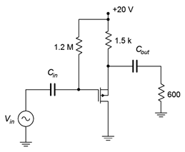
Figure \(\PageIndex{8}\)
13.5.4: Computer Simulation Problems
17. Utili\(Z_{in}\)g manufacturer's data sheets, find devices with the following specifications (typical) and verify them using the measurement techniques presented in the prior chapter.
Device 1: \(V_{GS(off)}\) = −2 V, \(I_{DSS}\) = 25 mA.
Device 2: \(V_{GS(off)}\) = −1.5 V, \(I_{DSS}\) = 40 mA.
18. Using the device model from the preceding problem, verify the design of Problem 13.
19. Using the device model from Problem 17, verify the design of Problem 14.