
3.11: Problems
- Page ID
- 50372

1.
(a) A 1nm × 1nm molecule is 30Å away from a metal contact. Calculate the electrostatic capacitance using the parallel plate model of the capacitor. Find the change in potential per charge added to the molecule, \(U_{ES}/\delta n\).
(b) A 50nm × 50nm molecule is 30Å away from a metal contact. Calculate the electrostatic capacitance using the parallel plate model of the capacitor. Find the change in potential per charge added to the molecule, \(U_{ES}/\delta n\).
(c) A 100nm × 100nm molecule is 30Å away from a metal contact. Calculate the electrostatic capacitance using the parallel plate model of the capacitor. Find the change in potential per charge added to the molecule, \(U_{ES}/\delta n\).
2.
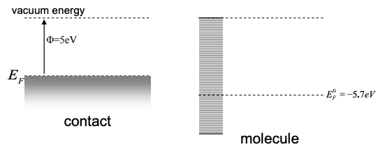
(a) Assume the molecule in problem 1(a) has a uniform density of states of \(g(E)=3\times 10^{20}/eV\) and Fermi level at \(E^{0}_{F} = -5.7eV\) in isolated space. The metal has a work function of 5eV. Sketch all of the energy levels in equilibrium after the metal contact and molecule are brought into contact. Find the number of charges, \(\delta_{n}\), transferred from the molecule to the metal (or vice versa.).
(b) Repeat part (a) for the molecule in problem 1(b) using the same density of states and Fermi levels.
(c) Repeat part (a) for the molecule in problem 1(c) using the same density of states and Fermi levels.
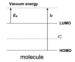
3. Consider the molecule illustrated below with \(E_{A}=2eV,\ I_{P}=5eV, \text{ and } E_{F}^{0}=3.5eV\).
(a) What is \(C_{Q}\) when the electron lifetime is \(\tau=\infty \), 1ps, 1fs?
(b) For each of the lifetimes in part (a), what is the equilibrium Fermi level when \(\delta n = 0.1\) charge is added to the molecule.
(c) What is the equilibrium Fermi level when \(\tau_{HOMO}=.1ps\) and \(\tau_{LUMO}=1ps\)?
4. A quantum well is brought into contact with a metal electrode as shown in the figure below.
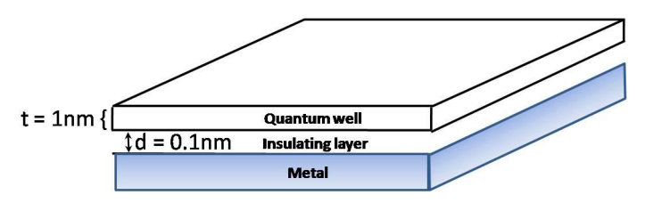
(a) Calculate the DOS in the well between 0 and 2eV assuming an infinite confining potential and that the potential inside the well is zero.
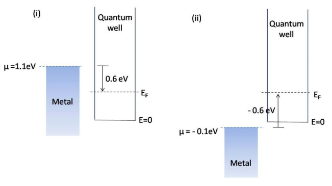
(b) On contact charge can flow between the metal and the quantum well. But assume that on contact the well is still separated from the metal by a 0.1nm thick layer with dielectric constant \(5\times8.84\times10^{-12}F/m\). Calculate the surface charge density at equilibrium, for an initial separation of (i) 0.6eV and (ii) -0.6eV, between the quantum well \(E_{F}\) and the chemical potential of the metal. Assume T=0.
(c) Plot the vacuum energy shift at each interface at equilibrium, for part b (i) and (ii), above.
The next question is adapted from an example in "Introductory Applied Quantum and Statistical Mechanics" by Hagelstein, Senturia and Orlando, Wiley Interscience 2004.
5. In this problem we consider charge injection from a discrete energy level rather than a metal. Consider charge transport through a quantum dot buried within an insulator. The materials are GaAs|GaAlAs|GaAs|GaAlAs|GaAs with thicknesses 1000Å|40Å|100Å|40Å|1000Å. The potential landscape of this device is modeled as below with \(V_{0}=0.3eV,\ b=50Å, \text{ and } a=90Å \). Let the effective mass of an electron in GaAs and GaAlAs be \(0.07m_{e}\), where \(m_{e}\) is the mass of an electron.
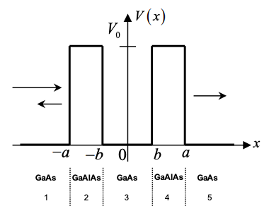
Considering only energies below V0, the wavefunction is piecewise continuous with
\( \left\{\begin{array}{l}
\psi_{1}=e^{i k x}+B e^{-i k x} \\
\psi_{2}=C e^{-\alpha x}+D e^{\alpha x} \\
\psi_{3}=F e^{i k x}+G e^{-i k x}, \text { where } k=\frac{\sqrt{2 m E}}{\hbar} \text { and } \alpha=\frac{\sqrt{2 m\left(V_{0}-E\right)}}{\hbar} \\
\psi_{4}=H e^{-\alpha x}+I e^{\alpha x} \\
\psi_{5}=J e^{i k x}
\end{array}\right. \)
(a) Match the boundary conditions and find \(\overline{\overline{M}}\) such that \(\overline{\overline{M}} \overline{C} = \overline{A}\), where
\( \bar{C}=\left(\begin{array}{c}
B \\
C \\
D \\
F \\
G \\
H \\
I \\
J
\end{array}\right) \text { and } \bar{A}=\left(\begin{array}{c}
e^{-i k a} \\
i k e^{-i k a} \\
0 \\
0 \\
0 \\
0 \\
0 \\
0
\end{array}\right) \)
(b) The transmission coefficient is \(T=|J|^{2}=|\overline{C}(8)|^{2}\), where \(\overline{C} = \overline{\overline{M}}^{-1}\overline{A}\). Determine T numerically or otherwise. It is plotted below as a function of electron energy, E. Verify that the resonant energies where T = 1 are within a factor of two of the eigenenergies of an infinite square well with width L=2b. Note that this approximation for the resonant energies works better for deeper square wells (\(V_{0}\) big).
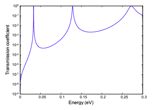
(c) Why do the widths of the resonances in the transmission coefficient increase at higher electron energy?
(d) Now suppose we apply a voltage across this device. Electrons at the bottom of the conduction band \(E_{C}\) in the GaAs on the left side will give net current flow which is proportional to the transmission coefficient T.
Let's first consider only one discrete energy level \(E_{0}\) in the dot as shown in part (a) of the figure below. Assume the potential drop is linear (electric field F is constant) across the whole device, as shown in part (b) of the figure below.
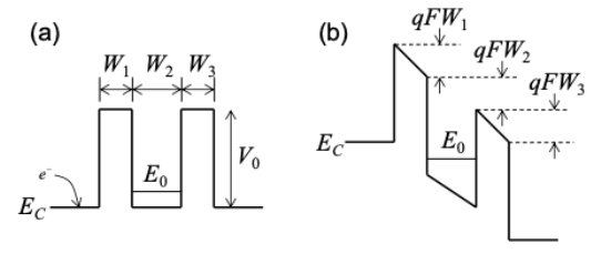
Sketch out qualitatively what you think the current-vs-voltage curve will look like. It should look quite different to the IV characteristic of a quantum dot with metal contacts. Explain the difference.
(e) Approximating \(E_{0}\) as the ground state of an infinite square well, what is the expression for the resonant voltage in terms of \(W_{2}\), assuming \(W_{1}=W_{3}\)?
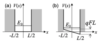
(f) Without solving for the wavefunction, sketch qualitatively what the probability density of the lowest eigenstate of an infinite well will look like when distorted by an electric field. Where in the well has the highest probability of finding an electron?
(g) Now, if we consider the multiple discrete energy levels in the dot, what will the current-voltage curve look like?
(h) Analytically determine the current through the dot at the 0.27eV resonance. Hint: consider the width of the resonance.
6. Consider the two terminal molecular device shown below. Note that this calculation differs from the previous calculation of charging by considering transport through the HOMO rather than the LUMO.
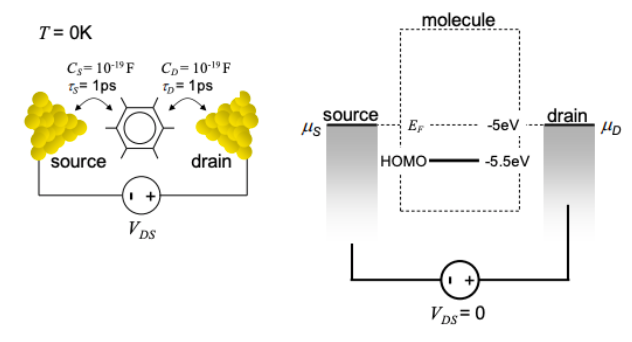
(a) Estimate the width of the HOMO from \(\tau_{S}\) and \(\tau_{D}\).
(b) Assuming that the molecule can be modeled as a point source conductor of radius 2nm, calculate the charging energy per electron. Compare to the charging energy determined from the capacitance values shown in Figure 3.11.9.
(c) Assuming that the charging energy is negligible, calculate the \(I_{DS}-V_{DS}\) characteristic and plot it.
(d) Now consider charging with \(q^{2}/C_{ES} = 1eV\). How does charging alter the maximum current and turn on voltage (the lowest value of \(V_{DS}\) when current flows)?
(e) Show that the number of electrons on the HOMO is at least
\(N=2\frac{\tau_{D}}{\tau_{S}+\tau_{D}}\)
(f) What is the maximum charging energy when \(q^{2}/C_{ES} = 1eV\)?
(g) Assuming that the charging energy is negligible, plot the energy level of the HOMO together with the source and drain workfunctions for \(V_{DS} = 2V\). On the same plot, indicate the energy level of the HOMO when \(q^{2}/C_{ES} = 1eV\) and \(V_{DS} = 2V\). What is the charging energy at this bias?
(h) Calculate the \(I_{DS}-V_{DS}\) characteristic when \(q^{2}/C_{ES} = 1eV\). Plot it on top of the \(I_{DS}-V_{DS}\) characteristic calculated for negligible charging.
7. Consider the two terminal molecular device shown in the figure below. This question considers conduction through both the HOMO and LUMO as well as the effect of mismatched source and drain injection rates and capacitances.
Note that: T = 0K; \(C_{S} = 2C_{D}\) ; \(\tau_{S} = 1ps\) ; \(\tau_{D} = 9ps\)
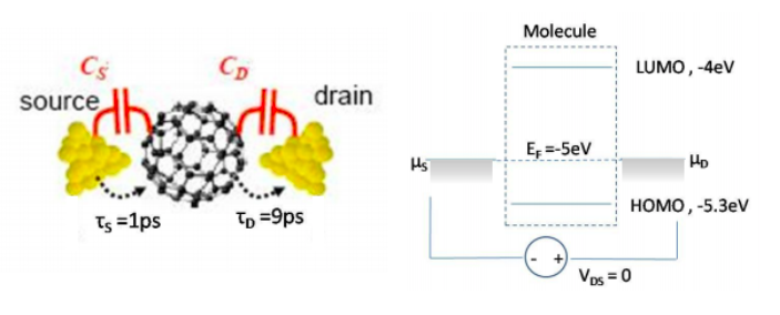
(a) Estimate the width of the HOMO and LUMO from \(\tau_{S}\) and \(\tau_{D}\).
(b) If \(C_{D} = 1pF\) calculate the charging energy per electron.
(c) Plot the current-voltage characteristic (IV) from \(V_{DS} = -10V\) to \(V_{DS} = 10V\) assuming that the charging energy equals zero.
(d) Assume the charging energy is now 1eV per electron. What is \(C_{D}\)?
(e) Plot the IV from \(V_{DS} = 0V\) to \(V_{DS} = 10V\) assuming that the charging energy is 1eV per electron.
(f) Plot the IV from \(V_{DS} = -10V\) to \(V_{DS} = 0V\) assuming that the charging energy is 1eV per electron. Hint: you should find a region of this IV characteristic in which the HOMO and LUMO are charging together, increasing the current but leaving the net charge on the molecule unchanged. Consequently, your IV characteristic should exhibit a step change in current at a particular voltage.
8. A quantum wire with square cross-section with a 1-nm thickness side is bent and fused into a circular ring with radius R= 2nm as shown below.
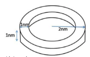
(a) Plot the DOS in the wire from E = 0 to E = 0.8eV. Assume an infinite confining potential and that the potential in the ring is V = 0.
(b) Next the ring is placed between contacts as shown. What is the charging energy?
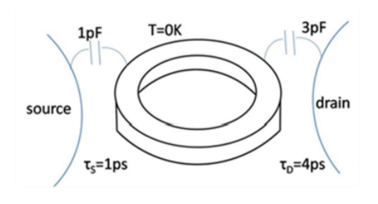
(c) Plot the current versus voltage for V from 0 to 1.1V.
(d) A magnetic field is applied perpendicular to the ring. Sketch the changes in the IV.
The next three questions have been adapted from F. Zahid, M. Paulsson, and S. Datta, "Electrical conduction in molecules". In Advanced Semiconductors and Organic Nanotechniques, ed. H. Korkoc. Academic Press (2003).
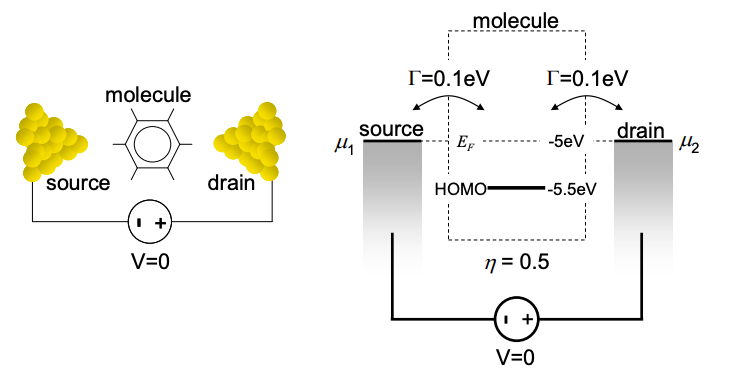
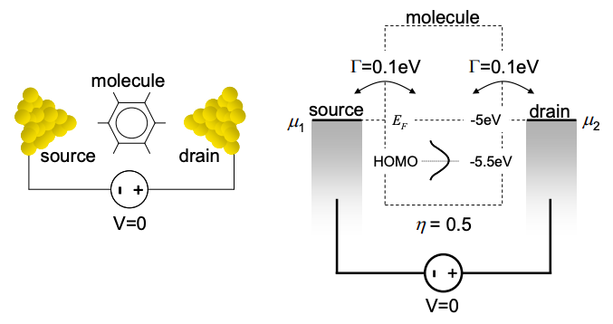
9.
(a) Numerically calculate the current-voltage and conductance-voltage characteristics for the system shown in Figure 3.11.13 with the following parameters:
\(\eta = 0.5 \\
E_{F}=-0.5\ eV \\
HOMO = -5.5\ eV \\
\Gamma_{S} = \Gamma_{D} = 0.1 eV \\
T = 298K\)
Set the charging energy to zero, i.e. take \(C_{ES} \rightarrow \infty\).
Hints
(1) Despite the statement that \(\Gamma_{S} = \Gamma_{D} = 0.1\ eV\), the HOMO in this problem is assumed to be infinitely sharp. Simplify Equations (3.7.7) and (3.7.8) for \(g(E-U)=2\delta (E-U-\epsilon)\), where \(\epsilon\) is the energy of the HOMO.
(2) You will need to implement the flow chart shown in Figure 3.7.4. If your solution for U oscillates and does not converge, try setting \(U=U_{old}+\alpha(U_{calc}-U_{old})\), where \(U_{calc}\) is the solution to Equation (3.6.6), \(U_{old}\) is the previous iteration's estimate of U and \(\alpha\) is a small number that may be reduced to obtain convergence.
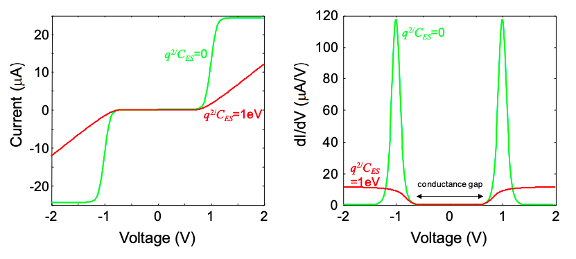
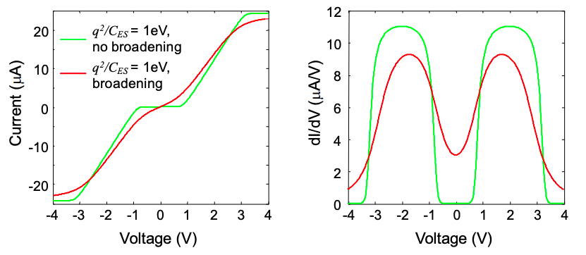
(b) Repeat the numerical calculation of part (a) with \(q^{2}/C_{ES} = 1\ eV\).
(c) Explain the origin of the conductance gap. What determines its magnitude?
(d) Write an analytic expression for the maximum current when \(q^{2}/C_{ES} = 0\).
(e) Explain why the conductance is much lower when the charging energy is non-zero.
10. Next, we add a LUMO level at -1.5 eV.
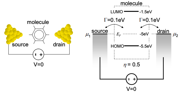
(a) Numerically calculate the current-voltage and conductance-voltage characteristics for \(q^{2}/C_{ES} = 1\ eV\) and \(E_{F} = -2.5\ eV\).
(b) Repeat the numerical calculation for \(q^{2}/C_{ES} = 1\ eV\) and \(E_{F} = -3.5\ eV\).
(c) Repeat the numerical calculation for \(q^{2}/C_{ES} = 1\ eV\) and \(E_{F} = -5.0\ eV\) (same as Q8.b).
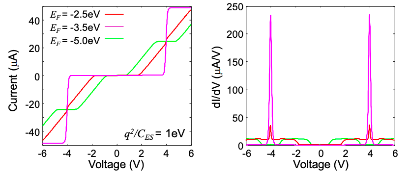
(d) Why are the current-voltage characteristics uniform? Hint: what would happen if \(\eta \neq 0.5\)? Identify the origin of the transitions in the IV curve.
(e) Why is the effect of charging absent when \(E_{F} = -3.5\ eV\)?
11. Next, we consider a Lorentzian density of states rather than simply a discrete level.
\[ g(E)dE = \frac{1}{\pi}\frac{\Gamma}{(E - \epsilon)^{2}+(\Gamma/2)^{2}}dE \nonumber \]
where \(\Gamma=\Gamma_{S}+\Gamma_{D}\) and \(\epsilon\) is the center of the HOMO. Ignore the LUMO, i.e. consider the system from Problem 9.
(a) Numerically compare the current-voltage and conductance-voltage characteristics for a discrete and broadened HOMO with \(q^{2}/C_{ES} = 1\ eV\).
(b) How would you expect the IV to change if \(\Gamma_{S} > \Gamma_{D}\)? Explain.
12. The following problem considers a 2-terminal conductor under illumination. The light produces an electron transfer rate of \(\alpha N_{H}\) from the HOMO to the LUMO. The light also causes an electron transfer rate of \(\alpha N_{L}\) from the LUMO to the HOMO, where \(\alpha\) is proportional to the intensity of the illumination, and the electron populations in the LUMO and HOMO are \(N_{L}\) and \(N_{H}\), respectively.
Assume \(C_{S} = C_{D}\), that the LUMO and HOMO are delta functions, and T = 300K. Also, assume that under equilibrium in the dark, the Fermi Energy is midway between the HOMO and LUMO.
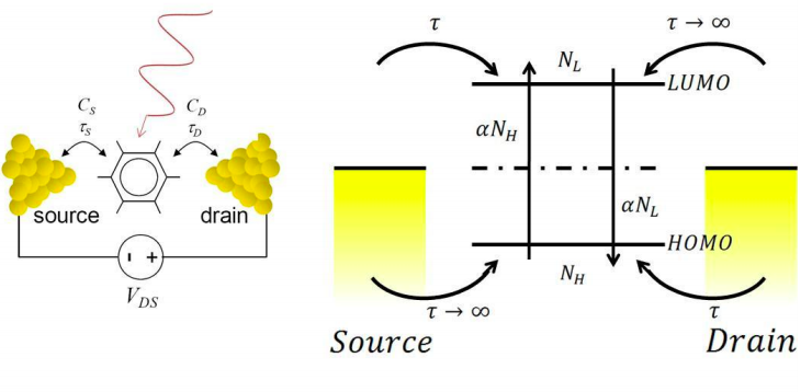
Next, imagine that the contacts are engineered to have the following characteristics:
Transfer rate between Drain and HOMO = \(1/\tau\).
Transfer rate between Drain and LUMO = 0.
Transfer rate between Source and HOMO = 0.
Transfer rate between Source and LUMO = \(1/\tau\).
(a) Determine the short circuit current for this system. (i.e. let \(V_{DS} = 0\), what is the current that flows through the external short circuit?)
(b) Determine the open circuit voltage for this system. (i.e. Disconnect the voltage source, what is the voltage that appears across the terminals of the molecule?)
(c) Repeat (a) and (b) with the addition of an additional electron transfer rate \(\beta N_{L}\) from the LUMO to the HOMO, where \(\beta\) is independent of the intensity of the illumination.
13. This problem refers to the 2 terminal molecular conductor below.
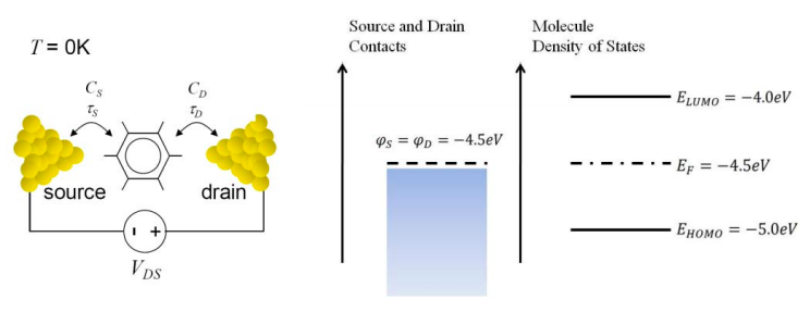
(a) When \(\tau_{s}=10 \text{ fs}\), \(\tau_{D}=5 \text{ fs}\), calculate the actual molecular density of states versus energy. Determine the full width half maximum of HOMO and LUMO.
(b) Based on the actual density of states calculated in part c), find the number of electrons and the charging energy when the molecule is brought into contact with the metal electrode and reached equilibrium (no applied voltage). Also sketch the energy diagram at equilibrium. Assume that the charging energy per electron is 1eV and \(\tau_{s}=10 \text{ fs}\), \(\tau_{D}=5 \text{ fs}\).
Hint: You will need your calculator to solve this. You might use \(\int \frac{1}{1+x^{2}}dx = tan^{-1}(x)\).