5.1: Field Effect Transistors
- Page ID
- 49992

Field Effect transistors (FETs) are the backbone of the electronics industry. The remarkable progress of electronics over the last few decades is due in large part to advances in FET technology, especially their miniaturization, which has improved speed, decreased power consumption and enabled the fabrication of more complex circuits. Consequently, engineers have worked to roughly double the number of FETs in a complex chip such as an integrated circuit every 1.5-2 years; see Figure 5.1.1 in the Introduction. This trend, known now as Moore's law, was first noted in 1965 by Gordon Moore, an Intel engineer. We will address Moore's law and its limits specifically at the end of the class. But for now, we simply note that FETs are already small and getting smaller. Intel's latest processors have a source-drain separation of approximately 65nm.
In this section we will first look at the simplest FETs: molecular field effect transistors. We will use these devices to explain field effect switching. Then, we will consider ballistic quantum wire FETs, ballistic quantum well FETs and ultimately non-ballistic macroscopic FETs.
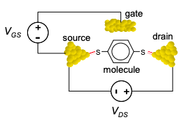
Molecular FETs
The architecture of a molecular field effect transistor is shown in Figure 5.1.1. The molecule bridges the source and drain contact providing a channel for electrons to flow. There is also a third terminal positioned close to the conductor. This contact is known as the gate, as it is intended to control the flow of charge through the channel. The gate does not inject charge directly. Rather it is capacitively coupled to the channel; it forms one plate of a capacitor, and the channel is the other. In between the channel and the conductor, there is a thin insulating film, sometimes described as the 'oxide' layer, since in silicon FETs the gate insulator is made from SiO2. In the device of Figure 5.1.1, the gate insulator is air.