Engineering LibreTexts

5.7: The Strong Charging Limit

  • Page ID
    51618
  • \( \newcommand{\vecs}[1]{\overset { \scriptstyle \rightharpoonup} {\mathbf{#1}} } \) \( \newcommand{\vecd}[1]{\overset{-\!-\!\rightharpoonup}{\vphantom{a}\smash {#1}}} \)\(\newcommand{\id}{\mathrm{id}}\) \( \newcommand{\Span}{\mathrm{span}}\) \( \newcommand{\kernel}{\mathrm{null}\,}\) \( \newcommand{\range}{\mathrm{range}\,}\) \( \newcommand{\RealPart}{\mathrm{Re}}\) \( \newcommand{\ImaginaryPart}{\mathrm{Im}}\) \( \newcommand{\Argument}{\mathrm{Arg}}\) \( \newcommand{\norm}[1]{\| #1 \|}\) \( \newcommand{\inner}[2]{\langle #1, #2 \rangle}\) \( \newcommand{\Span}{\mathrm{span}}\) \(\newcommand{\id}{\mathrm{id}}\) \( \newcommand{\Span}{\mathrm{span}}\) \( \newcommand{\kernel}{\mathrm{null}\,}\) \( \newcommand{\range}{\mathrm{range}\,}\) \( \newcommand{\RealPart}{\mathrm{Re}}\) \( \newcommand{\ImaginaryPart}{\mathrm{Im}}\) \( \newcommand{\Argument}{\mathrm{Arg}}\) \( \newcommand{\norm}[1]{\| #1 \|}\) \( \newcommand{\inner}[2]{\langle #1, #2 \rangle}\) \( \newcommand{\Span}{\mathrm{span}}\)\(\newcommand{\AA}{\unicode[.8,0]{x212B}}\)

    In metals and many large transistors in the ON state, the density of states at the Fermi level is sufficiently large that adding charges barely moves the channel potential. We say that the Fermi level is pinned. In the limit that \(g(E_{F}) \rightarrow \infty\) then \(\Delta U \rightarrow 0\).

    In terms of the quantum capacitance, we find that if \(C_{Q} \gg C_{ES}\), Equation (5.4.5) reduces to

    \[ q \delta N = \delta V_{GS}C_{G} \nonumber \]

    This limit is also known as strong inversion in conventional FET analysis. The channel transforms from an insulator to a metal. The transition occurs when the gate bias equals the threshold voltage, \(V_{T}\), which is defined as the gate bias required to push the channel energy level down to the source workfunction.

    In the strong charging/metallic limit, the gate and channel act as two plates of a capacitor. The charge in the channel then changes linearly with additional gate bias. In FETs, the channel potential relative to the source, \(V(x)\), may also vary with position. Including the channel potential and the threshold voltage in Equation \ref{5.7.1} yields:

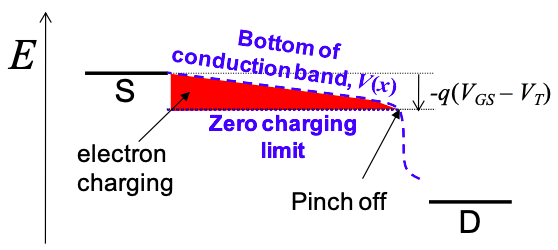
    One way to interpret the metallic limit is to consider the difference between the actual position of the conduction band edge and its position in the absence of charging. The difference is proportional to the amount of charging; see Figure \(\PageIndex{1}\). Note that the shaded region in the figure does not represent filled electron states below the conduction band. These electrons are in fact all at the bottom of the conduction band. Rather this the same graphical tool that we used in Part 3 to analyze charging within conductors.

    The metallic or strong inversion limit is only maintained for \(V_{GS}-V_{T}-V(x)>0\). If V(x) crosses the zero charging limit \((V_{GS}-V_{T})\) then charging decreases to zero. This is known as "pinch off".

    Screenshot 2021-05-18 at 18.18.51.png
    Figure \(\PageIndex{1}\): Charging opposes gateinduced changes in the channel potential. Here we illustrate the effect of charging in a non-ballistic FET. In the absence of charging, increasing gate potential lowers the conduction band edge (the "zero charging limit"). Charging pushes the conduction band edge back up towards the source workfunction. The red shaded region is the difference between the actual channel potential and the zero charging limit. It represents the population of electrons in the conduction band. It does not represent filled states below the bottom of the conduction band.

    This page titled 5.7: The Strong Charging Limit is shared under a CC BY-NC-SA 4.0 license and was authored, remixed, and/or curated by Marc Baldo (MIT OpenCourseWare) via source content that was edited to the style and standards of the LibreTexts platform; a detailed edit history is available upon request.