
5.15: Problems
- Page ID
- 51688
1. Buckyball FETs
Park et al. have reported measurements of a buckyball (C60) FET. An approximate model of their device is shown in Figure 5.15.1. The measured conductance as a function of \(V_{DS}\) and \(V_{GS}\) is shown in Fig. 5.15.2.
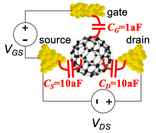
(a) Calculate the conductance \((dI_{DS}/dV_{DS})\) using the parameters in Figure 5.15.1. Consider \(5V<V_{GS}<8V\) calculated at intervals of 0.2V and \(-0.2V<V_{DS}<0.2V\) calculated at intervals of 10mV.
(b) Explain the X-shape of the conductance plot.
(c) Note that Park, et al. measure a non-zero conductance in the upper and lower quadrants. Sketch their \(I_{DS}-V_{DS}\) characteristic at \(V_{GS} ~ 5.9V\). Compare to your calculated \(I_{DS}-V_{DS}\) characteristic at \(V_{GS} ~ 5.9V\). Propose an explanation for the non-zero conductances measured in the experiment in the upper and lower quadrants.
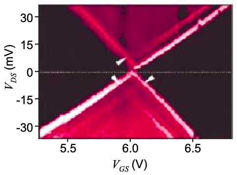
(d) In Park et al.'s measurement the conductance gap vanishes at \(V_{GS} = 6.0V\). Assuming that \(C_{G}\) is incorrect in Figure 5.15.1, calculate the correct value.
Reference
Park, et al. “Nanomechanical oscillations in a single C60 transistor” Nature 407 57 (2000)
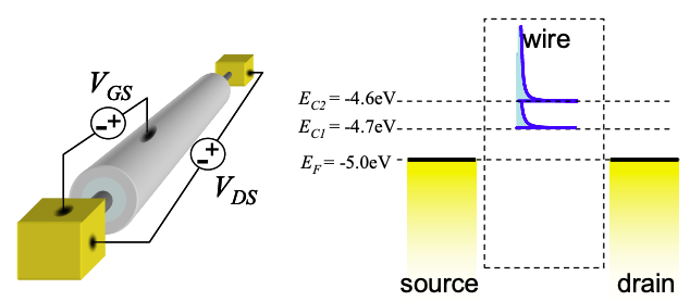
2. Two mode Quantum Wire FET
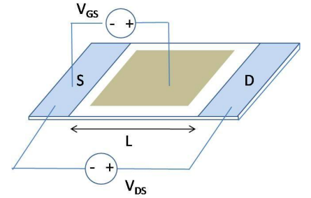
Consider the Quantum Wire FET of Fig. 5.17 in the text.
Assume that the quantum wire has two modes at \(E_{C1} = -4.7eV\), and \(E_{C2} = -4.6eV\). Analytically determine the \(I_{DS}-V_{DS}\) characteristics for varying \(V_{GS}\) at T = 0K. Sketch your solution for \(0<V_{DS}<0.5\), at \(V_{GS}\) = 0.3 V, 0.35 V, 0.4V, 0.45V and 0.5V.
Highlight the difference in the IV characteristics due to the additional mode.
3. 2-d ballistic FET
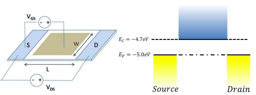
(a) Numerically calculate the current-voltage characteristics of a single mode 2-d ballistic FET using Equation (5.13.5) and a self consistent solution for the potential, U. Plot your solution for T = 1K and T = 298K. In each plot, consider the voltage range \(0<V_{DS}<0.5\), at \(V_{GS}\) = 0.3 V, 0.35 V, 0.4V, 0.45V and 0.5V. In your calculation take the bottom of the conduction band to be -4.7 eV, the Fermi Energy at equilibrium \(E_{F} = -5.0 eV\), L = 40nm, W = 3 × L, and \(C_{G} = 0.1 fF\). Assume \(C_{D} = C_{S} = 0\). Take the effective mass, m, as \(m = 0.5 \times m_{0}\), where \(m_{0} = 9.1\times10^{-31} kg\).
You should obtain the IV characteristics shown in Figure 5.13.1.
(b) Next, compare your numerical solutions to the analytic solution for the linear and saturation regions (Equations (5.13.12) and (5.13.13)). Explain the discrepancies.
(c) Numerically determine \(I_{DS}\) vs \(V_{GS}\) at \(V_{DS}= 0.5V\) and T = 298K. Plot the current on a logarithmic scale to demonstrate that the transconductance is 60mV/decade in the subthreshold region.
(d) Using your plot in (c), choose a new \(V_{T}\) such that the analytic solution for the saturation region (Equation (5.13.13)) provides a better fit at room temperature. Explain your choice.
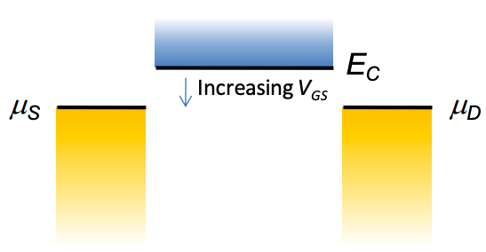
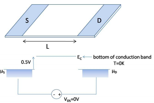
4. An experiment is performed on the channel conductor in a three terminal device. Both the source and drain are grounded, while the gate potential is varied. Assume that \(C_{G} \gg C_{S},\ C_{D}\).
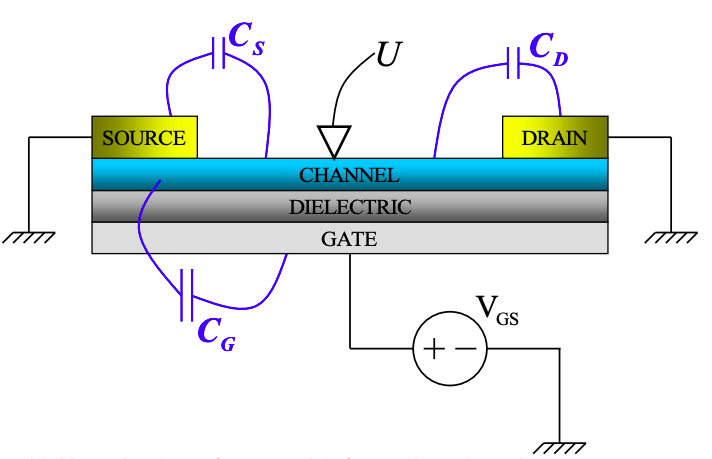
The transistor is biased above threshold \((V_{GS} > V_{T})\). Measurement of the channel potential, U, shows a linear variation with increasing \(V_{GS} > V_{T}\).
Under what conditions could the conductor be:
(i) a quantum dot (0 dimensions)?
(ii) a quantum wire (1 dimension)?
(iii) a quantum well (2 dimensions)?
Explain your answers.
5. Consider a three terminal molecular transistor.
(a) Assume the molecule contains only a single, unfilled molecular orbital at energy D above the equilibrium Fermi level. Assume also that \(C_{G} \gg C_{S},\ C_{D}\) and \(\Delta \gg kT\). Calculate the transconductance for small \(V_{DS}\) as a function of T and \(V_{GS}\) for \(V_{GS} \ll \Delta\).
Express your answer in terms of \(I_{DS}\).
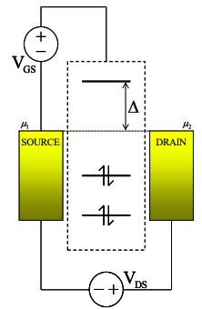
(b) Now, assume that the density of molecular states is
\[ g(E) = \frac{1}{E_{T}} \text{exp}\left[ \frac{E-\Delta}{E_{T}} \right] u(\Delta - E) \nonumber \]
where \(E_{T} \gg kT\). Calculate the transconductance for small \(V_{DS}\) as a function of T and \(V_{GS}\) for \(V_{GS} \ll \Delta\). Assume \(C_{G} \rightarrow \infty\).
Express your answer in terms of \(I_{DS}\).
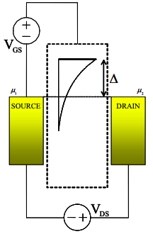
(c) Discuss the implications of your result for molecular transistors.
6. Consider the conventional n-channel MOSFET illustrated below:
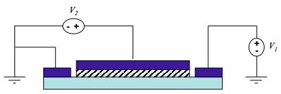
Assume \(V_{T} = 1V\) and \(V_{2} = 0V\). Sketch the expected IV characteristics (I vs. \(V_{1}\)) and explain, with reference to band diagrams, why the IV characteristics are not symmetric.
7. Consider a ballistic quantum well FET at T = 0K.
Recall that the general solution for a quantum well FET in saturation is:
\[ I_{DS} = \frac{qW}{\pi^{2}\hbar^{2}}\sqrt{\frac{8m}{9}} (\eta q (V_{GS-V_{T}}))^{3/2} \nonumber \]
(a) In the limit that \(C_{Q} \gg C_{ES}\), the bottom of the conduction band, \(E_{C}\), is "pinned" to \(\mu_{S}\) at threshold. Show that under these conditions \(\eta \rightarrow 0\).
(b) Why isn‟t the conductance of the channel zero at threshold in this limit?
(c) Given that \(C_{OX} = C_{G}/(WL)\), where W and L are the width and length of the channel, respectively, show that the saturation current in this ballistic quantum well FET is given by
\[ I_{DS} = \frac{8 \hbar W}{3m\sqrt{\pi q}}\left( C_{OX} \left( V_{GS}-V_{T} \right) \right)^{3/2} \nonumber \]
Hint: Express the quantum capacitance in the general solution in terms of the device parameters m, W, and L.
8. A quantum well is connected to source and drain contacts. Assume identical source and drain contacts.
(a) Plot the potential profile along the well when \(V_{DS} = +0.3V\).
Now a gate electrode is positioned above the well. Assume that, \(C_{G}\ggC_{S},\ C_{D}\) except very close to the source and drain electrodes. At the gate electrode \(\epsilon = 4 \times 8.84 \times 10^{-12}\ F/m\) and d = 10nm. Assume the source and drain contacts are identical.
(b) What is the potential profile when \(V_{DS} = 0.3V\) and \(V_{GS} = 0V\).
(c) Repeat (b) for \(V_{DS} = 0V\) and \(V_{GS} = 0.7V\). Hint: Check the \(C_{Q}\).
(d) Repeat (b) for \(V_{DS} = 0.3V\) and \(V_{GS} = 0.7V\) assuming ballistic transport.
(e) Repeat (b) for \(V_{DS} = 0.3V\) and \(V_{GS} = 0.7V\) assuming non-ballistic transport.
9. This problem considers a 2-d quantum well FET. Assume the following:
T = 0K, L = 40nm, W = 120nm, \(C_{G}\) = 0.1fF , \(C_{S} = C_{D} = 0\)
(a) Compare the operation of the 2-D well in the ballistic and semi-classical regimes.
Assume \(C_{Q} \rightarrow \infty \gg C_{ES}\) in both regimes.
Take \(\mu = 300\text{ cm}^{2}/Vs\) in the semi-classical regime.
Plot \(I_{DS}\) vs \(V_{DS}\) for \(V_{GS} = 0.5V\) and \(V_{DS} = 0 \text{ to } 0.5V\).
(b) Explain the difference in the IV curves. Is there a problem with the theory? If so, what?