
7.10: Problems
- Page ID
- 52428
Q1. Adiabatic Transistors
Consider the inverter shown below.
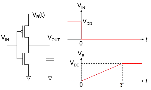
Unlike in a conventional CMOS inverter, in this device, the supply voltage, \(V_{R}\), adjusts during the switching operation. Initially the voltage on the output capacitor is zero, but at t = 0 the input voltage drops to zero. Also at t = 0, the supply voltage ramps from zero to the logic high voltage, \(V_{DD}\).
Assume that the PMOS FET is modeled by a resistor, R.
(a) Show that the energy dissipated during the switching operation is
\( E = \frac{RC}{\tau} CV_{DD}^{2} \text{ for } \tau \gg RC \)
This is known as an adiabatic switch, since switching occurs (in the limit) with no energy dissipation, i.e. we are adding charge to a capacitor using a vanishingly small excess voltage.
[Hint: You may assume \(V_{OUT}\) of the form \(V_{OUT} = a + b\exp[-t/RC] + ct\) where a, b, and c are constants to be determined.]
(b) Show also that the energy dissipated reduces to the standard CMOS switching energy \(E = \frac{CV_{DD}^{2}}{2} \text{ for } \tau \gg RC\)
(c) The above example shows adiabatic switching when the capacitor voltage changes from low to high. Can it be implemented generally? i.e. consider the case when the capacitor voltage changes from high to low. And what happens when the capacitor does not change voltage during a cycle?
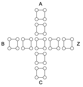
Q2. Cellular Automata
This question refers to a proposed architecture for molecular electronics: Molecular Quantum-Dot Cellular Automata. The figures are drawn from the reference.
In this architecture information is stored in bistable cells. An example cell is shown below:
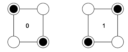
This cell consists of four electron traps positioned at the corners of a square. Only two of the traps are filled. From electrostatics, there are two stable states with the electrons at opposing corners of the square.
To transmit information, the cells are placed in a line. Information then propagates electrostatically, without current flow. It is argued that power dissipation is therefore eliminated and no interconnecting wires are required.
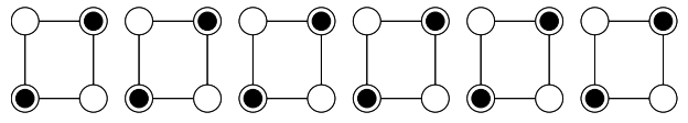
By changing the topology, it is possible to make logic gates. For example, below we show an inverter.
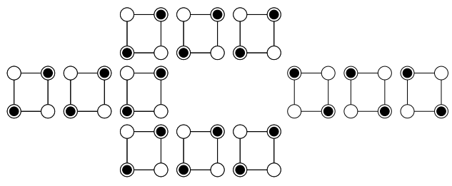
(a) A proposed "majority gate" is shown below. The output Z is the majority of the inputs, A, B and C. i.e. if there are more 1 inputs than zero inputs then Z = 1, otherwise Z = 0. Use this gate to design a two input AND gate.
(b) Is the majority gate truly dissipationless? Hint: calculate the entropy before and after a majority decision.
Reference: Lent, “Bypassing the transistor paradigm” Science 288 1597 (2004)
Q3. Power delay products at the nanoscale
The power delay product is the minimum energy dissipated per bit of information processed. For a CMOS inverter the PDP is:
\[ PDP = CV^{2} \nonumber \]
where V is the supply voltage and C is the load capacitance as seen by the inverter. In this question, we will assume that the supply voltage is fixed.
(a) Determine the load capacitance as a function of the gate and quantum capacitances. Assume we can neglect all other capacitances.
(b) Consider a 2d field effect transistor (where \(C_{Q} \rightarrow \infty\)). If its dimensions are scaled by a factor s, how does the PDP scale?
(c) Now consider a quantum wire field effect transistor with \(C_{Q}\ll C_{G}\). Its gate capacitance is given by
\[ C_{G}=2\pi \varepsilon \frac{l}{\log(r/a_{0})} \nonumber \]
where \(\varepsilon\) is the dielectic constant of the gate insulator, l is the gate length, r is the gate radius and \(a_{0}\) is the 1d wire radius.
Assume that l and r are scaled by a factor s, how does the gate capacitance for a quantum wire field effect transistor scale?
(d) Now consider the impact of the quantum capacitance on the PDP on the quantum wire field effect transistor. How does the overall PDP scale? Is the scaling faster or slower than the equivalent PDP using large quantum well field effect transistors?
Q4. Mechanical transistors
Consider a mechanical switch.
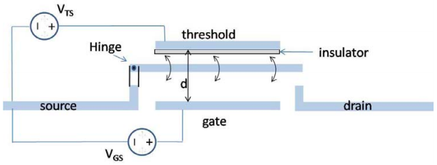
The conductor is pulled towards the gate electrode when \(|V_{GS}|>|V_{TS}|\), switching the device on, and towards the threshold electrode when \(|V_{GS}|<|V_{TS}|\) switching the device off. Assume two switches are wired together in a complementary logic circuit that drives a capacitive load as shown below.
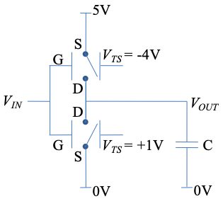
(i) Plot steady state \(V_{OUT}\) versus \(V_{IN}\), where \(V_{IN}\) ranges from 0 to 5V. Show that the circuit is complementary.
(ii) Assume \(V_{IN}\) is switched from 0V to 5V and then back to 0V. How much energy is dissipated?
(iii) Consider one of the switches. Let \(C_{T}^{ON}\) and \(C_{G}^{ON}\) be the threshold-conductor capacitance, and the gate-conductor capacitance, respectively, in the ON state, and let \(C_{T}^{OFF}\) and \(C_{G}^{OFF}\) be the capacitances, respectively, in the OFF state. See the figure below.
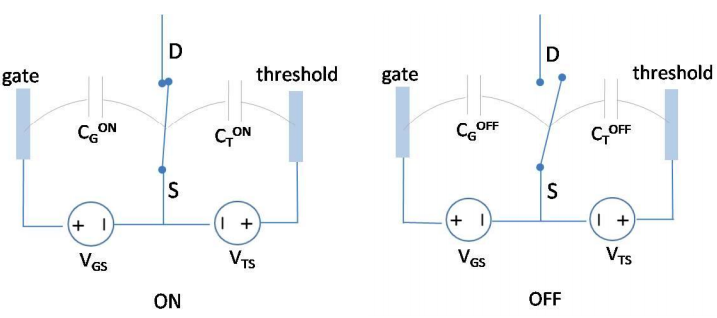
What is the energy stored in these capacitors in the (a) ON and in the (b) OFF positions as a function of \(V_{GS}\) and \(V_{TS}\)?
Now connect N switches all wired in parallel.
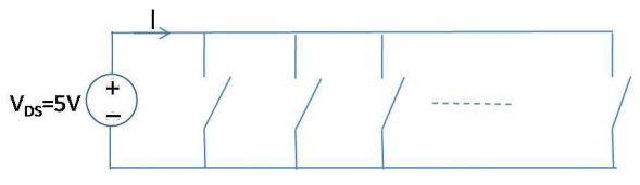
Each switch has \(V_{TS} = +1V\) and resistance, \(R=100\Omega\). Assume all the gate electrodes are wired together at a potential \(V_{GS}\). To simplify the analysis assume that \(C_{G}^{ON} \gg C_{T}^{ON}\) and also that \(C_{T}^{OFF} \gg C_{G}^{OFF}\). Furthermore, take \(C_{G}^{ON} = C_{T}^{OFF} = C\).
(iv) Considering Boltzmann statistics, and the potential energy difference between the OFF and ON states, out of the N switches, what is the probable number of switches that are ON as a function of C, \(V_{GS}\) and \(V_{TS}\) when \(|V_{GS}|<|V_{TS}|\)?
(v) Find I for the N switches as a function of \(V_{GS}\) and \(V_{TS}\) for \(0 < V_{GS} < 5V\) (for \(V_{TS} = 1V\)).
(vi) Does the mechanical switch exhibit any benefit over conventional CMOS?
Q5.
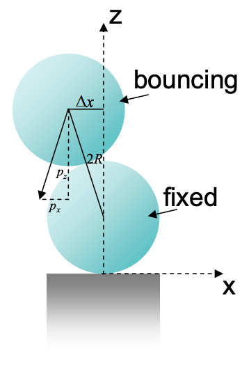
(a) Consider two identical balls each 1cm in diameter and of mass m = 1g. One is kept fixed, and the second is dropped directly on it from a height of d = 10cm. From the uncertainty principle alone, what is the expected number of times the moving ball bounces on the stationary ball before it misses the latter ball altogether? Assume the ball is dropped from an optimal initial state.
Hint: some parts of this problem can be solved classically.
(b) Discuss the implications of (i) for billiard ball computers.
Q6. The following question refers to ion channel mechanical switches at T = 300K.
a) Assume that any given ion channel is either open with conductance \(G = G_{0}\), or closed with conductance \(G = 0\). Using Boltzmann statistics, write an expression for the conductance of a giant squid axon (with N ion channels in parallel) as a function of the applied membrane potential, V. Assume that the number of open channels at \(V = 0\) is \(N_{0}\).
Hint: Given Boltzmann statistics, the relative populations \(N_{1}\) and \(N_{2}\) of two states separated by energy dU are \(N_{1}/N_{2} = \exp(-dU/kT)\).
b) Where possible given the data in Figure 7.5.8, evaluate your parameters.
c) Sketch a representative IV of a single ion channel.