
7.3: Scaling Limits in CMOS
- Page ID
- 52420
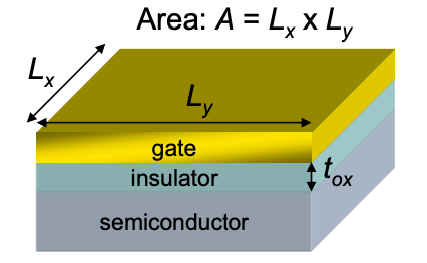
Equation \ref{7.2.4} demonstrates the importance of the gate capacitance. The capacitance is
\[ C = \frac{\varepsilon A}{t_{ox}} \nonumber \]
where A is the cross sectional area of the capacitor, \(t_{ox}\) is the thickness of the gate insulator and \(\varepsilon\) is its dielectric constant.
Now, if we scale all dimensions down by a factor s(s<1), the capacitance decreases:
\[ C(s) = \frac{\varepsilon s^{2} A}{st_{ox}} = sC_{0} \label{7.3.1} \]
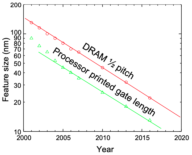
From Equation \ref{7.2.4}, reductions in C reduce the PDP, allowing circuits to run faster for a given power dissipation. Indeed, advances in the performance of electronics have come in large part through a continued effort of engineers to reduce the size of transistors, thereby reducing the capacitance and the PDP; see Figure \PageIndex{2}.
At present, however, there are increasing concerns that we are approaching the end of our ability to scale electronic components. There are at least two looming problems in electronics:
Poor electrostatic control
We saw in part 5 that gate control over charge in the channel requires \(t_{ox} \ll L\), where L is the channel length. Now as the channel length, \(L \rightarrow 10\ nm\), \(t_{ox} \rightarrow 1\ nm\), i.e. the gate insulator is only several atoms thick! But the electric field across the gate must remain high to induce charge in the channel. Thus, reductions in feature sizes will eventually place severe demands on the gate insulator.
Power density
The electrostatic problem is fundamental, but it is possible that power concerns may obstruct the scaling of CMOS circuits prior to the onset of electrostatic issues. Power density is a particular concern since it does not benefit from continued reductions in component size. If the dimensions of a MOSFET are scaled down by a factor s(s<1), \(C \propto s\) (recall that capacitance is proportional to cross sectional area, and inversely proportional to the spacing between the charges). But even if the PDP scales as s, the power density may increase because the number of devices per unit area increases as \(1/s^{2}\).
The power densities of typical integrated circuits are approaching those of a light bulb filament ( ~ 100 W/cm2 ). For comparison, the power density of the surface of the sun is ~ 6000 W/cm2 . Removal of the heat generated by an integrated circuit has become perhaps the crucial constraint on the performance of modern electronics. Indeed, the fundamental limit to power density appears to be approximately 1000 W/cm2 . In practice, using water cooling of a uniformly heated Si substrate with embedded micro channels, a power density of 790 W/cm2 has been achieved with a substrate temperature near room temperature.
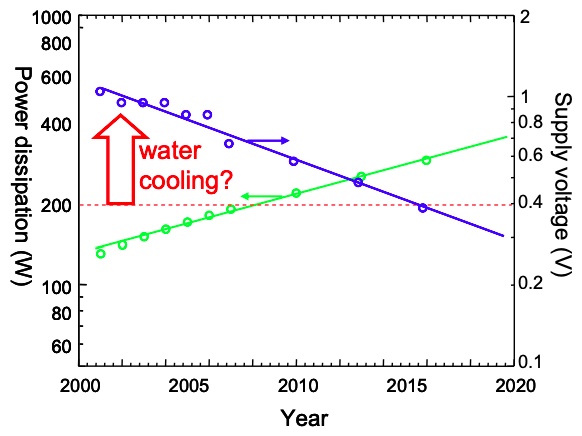
As is evident from Equation \ref{7.2.4} above, the PDP also depends on the supply voltage \(V_{DD}\). Ensuring that the total power dissipated per chip \ll 200 W has driven \(V_{DD}\) from 5V in early CMOS circuits to nearly 1V today. If the industry conforms to roadmap predictions, the supply voltage will eventually reach 0.4V by 2016.
But what is the ultimate limit to the PDP?