
9.3: Single Chip Oscillators and Frequency Generators
- Page ID
- 3602

The generation of signals is a basic requirement for a wide variety of applications, thus a number of manufacturers produce a selection of single IC oscillators and frequency generators. Some of these tend to work in the range below 1 MHz and usually require some form of external resistor/capacitor network to set the operating frequency. Other, highly specialized circuits for targeted applications are also available. In this section we shall examine a few of the ICs that are generically referred to as clock generators, voltage-controlled oscillators, phase-locked loops and timers.
9.3.1: Square Wave/Clock Generator
The need for stable, low cost, easy-to-use integrated circuits to generate square waves for clocking needs is widespread. Several companies manufacture such devices. One example is the LTC6900 from Linear Technology. A description sheet with a basic programming formula is shown in Figure \(\PageIndex{1}\).
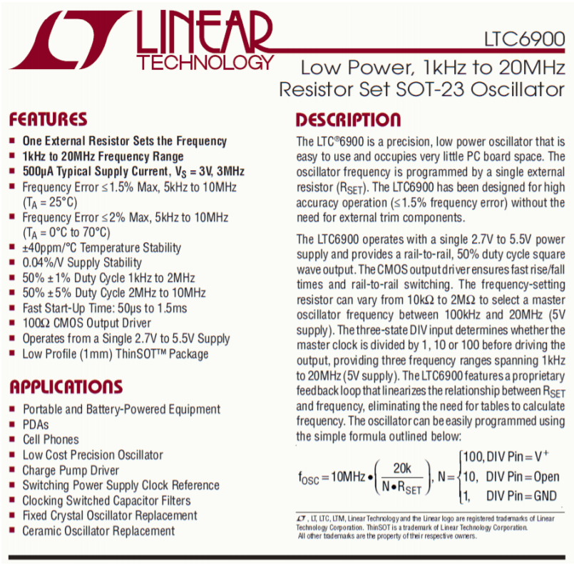
Figure \(\PageIndex{1}\): LTC6900 description. Reprinted courtesy of Linear Technology
The LTC6900 is a 5 volt low power circuit available in an SOT-23 (5 pin) package. It operates from 1 kHz to 20 MHz. The output frequency is programmable via a single resistor and the connection to its divider pin (labeled DIV). The frequency of the master oscillator is given by the equation
\[ f_o = 10 MHz \frac{20 k}{R_{set}} \label{9.33} \]
\(R_{set}\) is connected from the power supply pin to the SET pin. Acceptable values range between 10 k\(\Omega\) and 2 M\(\Omega\). If the DIV pin is grounded, the output frequency will be as calculated. If the DIV pin is left unconnected, the output frequency will be divided by 10 and if the DIV pin is connected to +5 volts, the output frequency will be reduced by a factor of 100. This is summarized graphically in Figure \(\PageIndex{2}\).
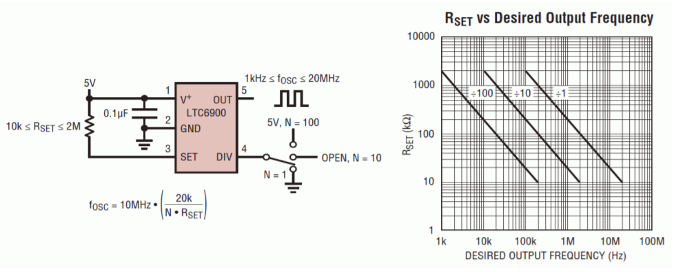
Figure \(\PageIndex{2}\): LTC6900 oscillator. operation Reprinted courtesy of Linear Technology
Example \(\PageIndex{1}\)
Using the LTC6900, design a 10 kHz square wave oscillator.
10 kHz is well within the range of this IC. To achieve this comfortably, we will need a divide-by-100 setting based on the graph of Figure \(\PageIndex{2}\). This will require us to tie the DIV pin to +5 volts. The value of \(R_{set}\) can be approximated from the graph or computed directly.
\[ f_{osc} = 10 MHz \frac{20 k}{N\times R_{set}} \nonumber \]
\[ R_{set} = 10 MHz \frac{20 k}{N\times f_{osc}} \nonumber \]
\[ R_{set} = 10 MHz \frac{20 k}{100\times 100 kHz} \nonumber \]
\[ R_{set} = 200 k \nonumber \]
9.3.2: Voltage-Controlled Oscillator
A voltage-controlled oscillator (usually abbreviated as VCO) does not produce a fixed output frequency. As its name suggests, the output frequency of a VCO is dependent on a control voltage. There is a fixed relationship between the control voltage and the output frequency. Theoretically, just about any oscillator can be turned into a VCO. For example, if a resistor is used as part of the tuning circuit, it could be replaced with some form of voltage-controlled resistor, such as an FET or a light-dependent resistor/lamp combination. By doing this, an external potential can be used to set the frequency of oscillation. This is very useful if the frequency needs to be changed quickly or accurately swept through some range.
A classic example of the usefulness of a VCO is shown in Figure \(\PageIndex{3}\). This is a simplified schematic of an analog monophonic musical keyboard synthesizer. The keys on the synthesizer are little more than switches. These switches tap potentials off a voltage divider. As the musician plays up the keyboard, the switches engage higher and higher potentials. These levels are used to control a very accurate VCO. The higher the control voltage, the higher the output frequency or pitch will be.
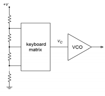
Figure \(\PageIndex{3}\): Simplified music synthesizer using VCO.
VCOs can be used for a number of other applications, including swept frequency spectrum analyzers, frequency modulation and demodulation, and control systems. It is also an integral part of the phase-locked loop, as we will see later in this chapter.
An example of a VCO is the LTC6990. It is part of Linear Technology's TimerBlox series of timer/counter/clock ICs. The series includes clock sources that operate in excess of 100 MHz and timers that switch at multi-hour rates. The LTC6990 operates in the range of just under 500 Hz to 2 MHz. While it can be used for fixed frequency applications, it also makes for a flexible VCO. An overview is shown in Figure \(\PageIndex{4}\).
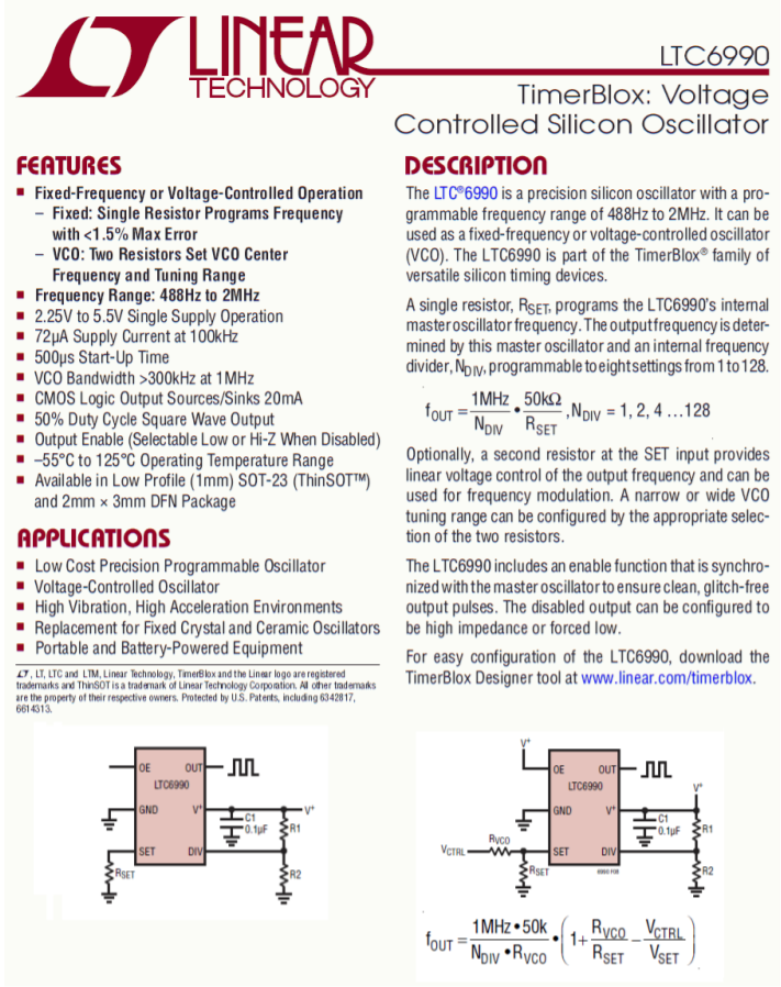
Figure \(\PageIndex{4}\): LTC6990 VCO. Reprinted courtesy of Linear Technology
Like the LTC6900, the LTC6990 is programmed with as little as one resistor and has a frequency divider option. Unlike its brother, the divider capabilities are much more broad, spanning eight power-of-two settings versus just three decade settings. A basic fixed frequency oscillator is shown at the bottom left of Figure \(\PageIndex{4}\) where the master oscillation frequency is controlled by \(R_{set}\). Standard VCO operation is shown at the bottom right. The LTC6990 also has the option of a high impedance output state, making a total of 16 divider/output possibilities. This set up is programmed typically through the use of two external resistors. The programming table is reproduced in Figure \(\PageIndex{5}\).
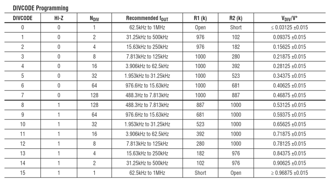
Figure \(\PageIndex{5}\): LTC6990 oscillator. programming Reprinted courtesy of Linear Technology
The output state depends on the combination of the Output Enable pin (OE) and the Hi-Z logic. When OE is high, the output will be active. If OE is low and Hi-Z is low, then the output will be held low. Finally, if OE is low and Hi-Z is high, then the output will go to a high impedance state.
The voltage present at the DIVCODE pin sets the frequency divider and the impedance mode. This voltage is interpreted by an internal 4 bit analog-to-digital converter (AD converters are the topic of Chapter Twelve). While it is possible to feed this pin with some external source, the more practical method is to simply create a voltage divider with a pair of 1% tolerance resistors; one tied from the power supply to the DIVCODE pin, and the second connected from DIVCODE to ground.
The master oscillator of the LTC6990 is controlled by the current at the SET pin. Internally, the voltage at this pin is maintained at 1 volt, therefore the frequency can be set by a single resistor, \(R_{set}\), connected from this pin to ground. It can then be divided down to lower frequency. This is essentially the same situation we found with the LTC6900. A 20 \(\mu\)A current (i.e., 50 k\(\Omega\)) will produce the top rate of 1 MHz. Lower currents (higher resistances) will produce proportionately lower frequencies.
The DIVCODE value will divide this base frequency down further by powers of two. We can express this relation with the following formula,
\[ f_{osc} = 1 MHz \frac{50 k}{N_{DIV} R_{set}} \label{9.34} \]
where \(N_{DIV}\) is found from the table in Figure \(\PageIndex{5}\)
The design process starts by identifying the appropriate frequency range. It is best if the desired oscillation frequency is not located at the extremes of any given range. Once a range is determined, the corresponding value for \(N_{DIV}\) is found, and along with it, the required divider resistor values, \(R_1\) and \(R_2\). From there it is a simple matter to solve Equation \ref{9.34} in terms of \(R_{set}\).
Example \(\PageIndex{2}\)
An LTC6990 is connected as shown in Figure \(\PageIndex{6}\). It is being used as a light-to-frequency converter. That is, the output frequency will be controlled by the amount of light hitting a sensor. The sensor is a CdS (Cadmium Sulfide) cell that is connected in the position of \(R_{set}\). Under low light conditions the cell will produce a high resistance and as the light level increases the resistance drops. Assuming that the cell varies from 500 k down to 60 k, determine the range of output frequencies. First, determine the DIVCODE value. This can be found by computing the voltage divider ratio of \(R_1\) and \(R_2\), but in this circuit recommended values have been used from the DIVCODE table. By observation, \(N_{DIV}=16\).
Next, we calculate the limit frequencies.
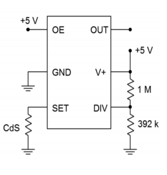
Figure \(\PageIndex{6}\): Light-to-frequency converter circuit for Example \(\PageIndex{2}\).
\[ f_{osc} = 1MHz \frac{50 k}{N_{DIV} R_{set}} \nonumber \]
\[ f_{osc} = 1MHz \frac{50k}{16\times 500 k} \nonumber \]
\[ f_{osc} = 6.25 kHz \nonumber \]
\[ f_{osc} = 1MHz \frac{50 k}{N_{DIV} R_{set}} \nonumber \]
\[ f_{osc} = 1MHz \frac{50k}{16 x 60 k} \nonumber \]
\[ f_{osc} = 52.08 kHz \nonumber \]
Note that as light levels increase, frequency increases in proportion.
When used in VCO mode, the most important element to remember is that the master oscillator frequency is set by the current coming out of the SET pin, \(I_{set}\), as expressed by the following formula
\[ f_o = 1 MHz \times 50 k \frac{I_{set}}{V_{set}} \nonumber \]
\(V_{set}\) is kept to 1 volt internally so this reduces to
\[ f_o = 1 MHz \times 50 k \times I_{set} \label{9.35} \]
\(f_{osc}\) is then divided down by \(N_{DIV}\). The final oscillation frequency may be expressed as
\[ f_{osc} = 1 MHz \times 50 k \frac{I_{set}}{N_{DIV}} \label{9.36} \]
Note that \(I_{set}\) is exiting the chip. Further, note the frequency of oscillation and \(I_{set}\) are directly proportional. Also, keep in mind that the \(I_{set}\) variation, and hence, the frequency variation, should be kept to 16:1 for best performance, where the maximum value of \(I_{set}\) is 20 \(\mu\)A. A simple method for obtaining voltage control is shown in Figure \(\PageIndex{4}\). There are some potential issues here. First, the range of voltage from the control circuit may not be able to achieve the desired frequency with that circuit. Second, note that higher control voltages will produce lower output frequencies, that is, an inverse relation. This can be an issue in some applications. Consequently, we shall examine a more generic method of controlling the circuit through the use of an external op amp for scaling and offsetting.
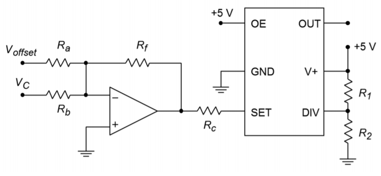
Figure \(\PageIndex{7}\): A method of mapping the control voltage.
The circuit of Figure \(\PageIndex{7}\) presents a method of mapping the existing control voltage onto the LTC6990 or any similar VCO. In this circuit a simple summing amplifier is used for scaling and offsetting. The control voltage, \(V_C\), is scaled by one channel of the weighted summer. This signal is offset by a DC voltage, \(V_{offset}\), fed through another channel. The voltage at the output of the op amp is used to sink current from the VCO via the control resistor, \(R_C\). Recall that the SET pin of the IC produces 1 volt internally and it is the exiting current, \(I_{set}\), that sets the master oscillator frequency, as expressed in Equation \ref{9.35}. Obviously, the op amp output voltage must be less than 1 volt in order for the op amp to sink current (i.e., in order for \(I_{set}\) to be exiting the LTC6990). The voltage difference between the op amp's output and the 1 volt at the SET pin drops across \(R_C\) and this is what creates \(I_{set}\). Note that as the control voltage grows more positive at the op amp's input, its output, and hence \(I_{set}\), also increases. Thus, frequency increases as control voltage increases.
Example \(\PageIndex{3}\)
Using Figure \(\PageIndex{7}\) as a guide, design a VCO circuit that will produce output frequencies from 20 kHz through 50 kHz when driven by control voltages from 6 to 8 volts (i.e., 6 volts will produce 20 kHz, 7 volts will produce 35 kHz, 8 volts will produce 50 kHz, etc.)
First, note that the frequency range is 2.5:1. As the LTC6990 can always cover any 8:1 span (as high as 16:1) and the maximum frequency of 50 kHz is well below the LTC6990's maximum, we know this IC is a good candidate for the design. We now need to determine the divider resistor values. Consulting Figure \(\PageIndex{5}\) shows that we can achieve this range using an \(N_{DIV}\) of 4, 8 or 16. Choosing the middle value, and assuming we don't care about Hi-Z state, we arrive at DIVCODE=3 with \(R_1\)=1 M\(\Omega\) and \(R_2\)=280 k\(\Omega\).
Our frequency range is 2.5:1 which means that our \(I_{set}\) range must also be 2.5:1. For convenience, choose the op amp's output to be 0 volts for the minimum frequency. This will yield 1 volt across \(R_C\) and occurs when the control voltage into the op amp is at its 6 volt minimum. When the control voltage is at its maximum of 8 volts we'll need 2.5 volts across \(R_C\) (i.e., 2.5 times the prior \(I_{set}\)). This means that the op amp's output must go to -1.5 volts. Note that a 2 volt change in the input control voltage will produce a 1.5 volt change at the op amp's output. Thus, the gain of this channel is -0.75. If we choose \(R_f\)=100 k\(\Omega\) then \(R_b\)=75 k\(\Omega\).
At this point we need to add an offset. With only the gain scaling, the 6 volt \(V_C\) produces -0.75 times 6, or -4.5 volts, and a \(V_C\) of 8 volts similarly produces -6 volts. Consequently, we need to add a +4.5 volt offset to the output. If we tie \(V_{offset}\) to the op amp's -15 volt power rail then we will need a gain of 4.5/(-15), or -0.3. With an \(R_f\) of 100 k\(\Omega\), \(R_a\) must be 333.3 k\(\Omega\) (the nearest 1% standard value is 332 k\(\Omega\)).
Finally, to determine \(R_C\), refer to Equation \ref{9.36} and solve for \(I_{set}\)
\[ I_{set} = \frac{f_{osc} \times N_{DIV}}{1 MHz \times 50 k} \nonumber \]
Using the minimum fosc of 20 kHz yields
\[ I_{set} = \frac{20 kHz \times 8}{1 MHz \times 50 k} \nonumber \]
\[ I_{set} = 3.2 \mu amps \nonumber \]
This occurs with 1 volt across \(R_C\). Therefore \(R_C\) = 312.5 k\(\Omega\). Crosschecking, when \(V_C\) = 8 V, we see 2.5 volts across \(R_C\) for a current of 8 \(\mu\)A. Inserting this into Equation \ref{9.36} yields 50 kHz, our desired maximum frequency.
In closing, note that the way in which the frequency sweeps depends on the wave shape of \(V_c\). If a sinusoid is used, the output frequency will vary smoothly between the stated limits. On the other hand, if the wave shape for \(V_c\) is a ramp, the output frequency will start at one extreme and then move smoothly to the other limit as the \(V_c\) ramp continues. When the ramp resets itself, the output frequency will jump back to its starting point. An example of this is shown in Figure \(\PageIndex{8}\). Finally, if the control wave shape is a square, the output frequency will abruptly jump from the minimum to the maximum frequency and back. This effect is shown in Figure \(\PageIndex{9}\), and can be used to generate FSK (frequency shift key) signals. FSK is used in the communications industry to transmit binary information.
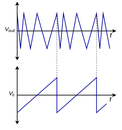
Figure \(\PageIndex{8}\): VCO frequency sweep using a ramp.
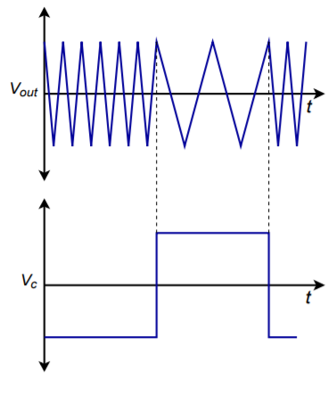
Figure \(\PageIndex{9}\): VCO two tone output using a square wave.
9.3.3: Phase-Locked Loop
One step up from the VCO is the Phase-Locked Loop, or PLL. The PLL is a selfcorrecting circuit; it can lock onto an input frequency and adjust to track changes in the input. PLLs are used in modems, for FSK systems, frequency synthesis, tone decoders, FM signal demodulation, and other applications. A block diagram of a basic PLL is shown in Figure \(\PageIndex{10}\).
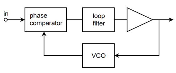
Figure \(\PageIndex{10}\): Phase-locked loop.
In essence, the PLL uses feedback in order to lock an oscillator to the phase and frequency of an incoming signal. It consists of three major parts; a phase comparator, a loop filter (typically, a lag network of some form), and a VCO. An amplifier may also exist within the loop. The phase comparator is driven by the input signal and the output of the VCO. It produces an error signal that is proportional to the phase difference between its inputs. This error signal is then filtered in order to remove spurious high-frequency signals and noise. The resulting error signal is used as the control voltage for the VCO, and as such, sets the VCO's output frequency. As long as the error signal is not too great, the loop will be selfstabilizing. In other words, the error signal will eventually drive the VCO to be in perfect frequency and phase synchronization with the input signal. When this happens, the PLL is said to be in lock with the input. The range of frequencies over which the PLL can stay in lock as the input signal changes is called the lock range. Normally, the lock range is symmetrical about the VCO's free-running, or center, frequency. The deviation from the center frequency out to the edge of the lock range is called the tracking range, and is therefore one-half of the lock range. This is illustrated in Figure \(\PageIndex{11}\).
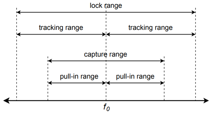
Figure \(\PageIndex{11}\): Operating ranges for phase-locked loop.
Although a PLL may be able to track changes throughout the lock range, it may not be able to initially acquire sync with frequencies at the range limits. A somewhat narrower band of frequencies, called the capture range, indicates frequencies that the PLL will always be able to lock onto. Again, the capture range is usually symmetrical about \(f_o\). The deviation on either side of \(f_o\) is referred to as the pull-in range. For a PLL to function properly, the input frequency must first be within the capture range. Once the PLL has locked onto the signal, the input frequency may vary throughout the larger lock range. The VCO center frequency is usually set by an external resistor or capacitor. The loop filter may also require external components. Depending on the application, the desired output signal from the PLL may be either the VCO's output, or the control voltage for the VCO.
One way to transmit binary signals is via FSK. This may be used to allow two computers to exchange data over telephone lines. Due to limited bandwidth, it is not practical to directly transmit the digital information in its normal pulse-type form. Instead, logic high and low can be represented by distinct frequencies. A square wave, for example, would be represented as an alternating set of two tones. FSK is very easy to generate. All you need to do is drive a VCO with the desired logic signal. To recover the data, the reception circuit needs to create a high or low level, depending on which tone is received. A PLL may be used for this purpose. The output signal will be the error signal that drives the VCO. The logic behind the circuit operation is deceptively simple. If the PLL is in lock, the output frequency of its VCO must be the same as the input signal. Remembering that the incoming FSK signal is itself derived from a VCO, for the VCOs to be in lock, they must be driven with identical control signals. Therefore, the control signal that drives the PLL's internal VCO must be the same as the control signal that originally generated the FSK signal. The PLL control signal can then be fed to a comparator in order to properly match the signal to the following logic circuitry.
Along the same lines as the FSK demodulator is the standard FM signal demodulator. Again, the operational logic is the same. In order for the PLL to remain in lock, its VCO control signal must be the same as the original modulating signal. In the case of typical radio broadcasts, the modulating signal is either voice or music. The output signal will need to be AC coupled and amplified further. The PLL serves as the intermediate frequency amplifier, limiter, and demodulator. The result is a very cost-effective system.
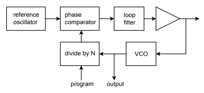
Figure \(\PageIndex{12}\): PLL frequency synthesizer.
Another usage for the PLL is in frequency synthesis. From a single, accurate signal reference, a PLL may be used to derive a number of new frequencies. A block diagram is shown in Figure \(\PageIndex{12}\). The major change is in the addition of a programmable divider between the VCO and the phase comparator. The PLL can only remain in lock with the reference oscillator by producing the same frequency out of the divider. This means that the VCO must generate a frequency \(N\) times higher than the reference oscillator. We can use the VCO output as desired. In order to change the output frequency, all that needs to be changed is the divider ratio. Normally, a highly accurate and stable reference, such as a quartz crystal oscillator, is used. In this way, the newly synthesized frequencies will also be very stable and accurate.
One example of an advanced digital PLL is the LTC6950. This device operates at up to 1.4 GHz and has five outputs. Each of the outputs has an independently programmable divider and VCO clock cycle delay. The input reference frequency is set between 2 MHz and 250 MHz. Due to the multiple outputs and syncing capabilities, this device can be used for large distributed systems that require precisely controlled multiple clocks. Indeed, one device can be used to control several other LTC6950s for very large systems. An example of this would be a system making use of several high-speed high-resolution analog-to-digital or digitalto-analog converters. The accuracy of these devices depends greatly on very accurate and stable clock sources. We will examine analog-to-digital-to-analog conversion in Chapter Twelve.
9.3.4: 555 Timer
The 555 timer is a versatile integrated circuit first introduced in the early 1970's by Signetics. It has remained a popular building block in a variety of applications ranging from simple square wave oscillators to burglar alarms to pulse-width modulators and beyond. In its most basic forms, the one-shot, or monostable, and the astable oscillator, the 555 requires only a handful of external components. Usually, only two capacitors and two resistors are needed for basic functions. The 555 is made by different manufacturers and in a few forms. The 556, for example, is a dual 555. The 555 can produce frequencies up to approximately 500 kHz. The output current is specified as 200 mA, although this entails fairly high internal voltage drops. A more reasonable expectation would be below 50 mA. The circuit may be powered from supplies as low as 5 volts and as high as 18 volts. This makes the 555 suitable for both TTL digital logic and typical op amp systems. Rise and fall times for the output square wave are typically 100 ns.
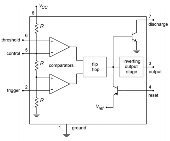
Figure \(\PageIndex{13}\): Block diagram of 555 timer.
A block diagram of the 555 is shown in Figure \(\PageIndex{13}\). It is comprised of a pair of comparators tied to a string of three equal-valued resistors. Note that the upper, or Threshold, comparator sees approximately 2/3 of \(V_{cc}\) at its inverting input, assuming no external circuitry is tied to the Control pin. (If the Control pin is unused, a 10 nF capacitor should be placed between the pin and ground.) The lower, or Trigger, comparator sees approximately 1/3 of \(V_{cc}\) at its noninverting input. These two comparators feed a flip-flop, which in turn feeds the output circuitry and Discharge and Reset transistors. If the flip-flop output is low, the Discharge transistor will be off. Note that the output stage is inverting, so that when the flip-flop output is low, the circuit output is high. In contrast, if the input to the Reset transistor is low, this will inhibit the output signal. If Reset capabilities are not needed, the Reset pin should be tied to \(V_{cc}\).
Returning to the comparators, if the noninverting input of the Threshold comparator were to rise above 2/3 \(V_{cc}\), the comparator's output would change state, triggering the flip-flop and producing a low out of the 555. Similarly, if the input to the inverting input of the Trigger comparator were to drop below 1/3 \(V_{cc}\), the comparator's output would change, and ultimately, the 555 output would go high.
9.3.5: 555 Monostable Operation
The basic monostable circuit is shown in Figure 9.39. In this form, the 555 will produce a single pulse of predetermined width when a negative going pulse is applied to the trigger input. Note that the three input components, \(R_{in}\), \(C_{in}\), and \(D\) serve to limit and differentiate the applied pulse. In this way, a very narrow pulse will result which reduces the possibility of false triggers. To see how the circuit works, refer to the waveforms presented in Figure 9.40.
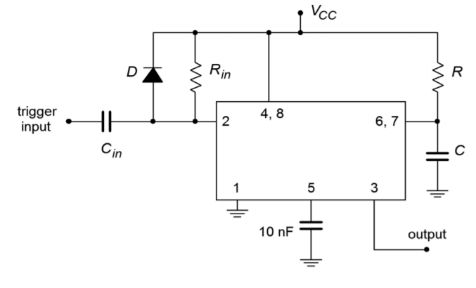
Figure \(\PageIndex{14}\): 555 monostable connection.
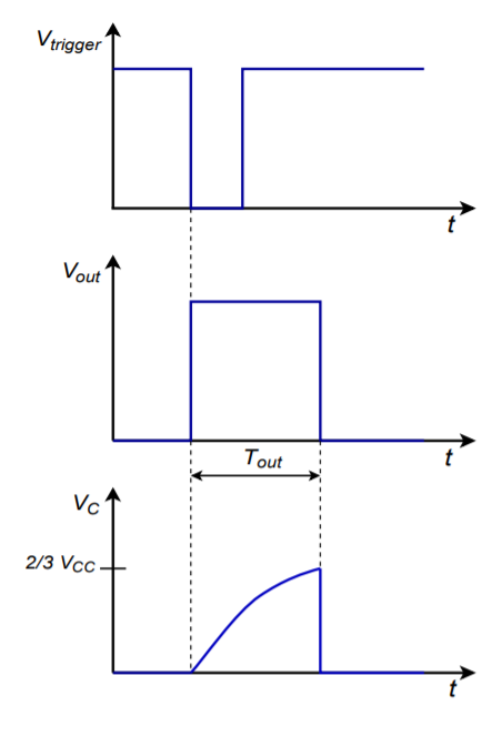
Figure \(\PageIndex{15}\): 555 monostable waveforms.
Assume that the output of the 555 is initially low. This implies that the Discharge transistor is on, shorting the timing capacitor \(C\). A narrow low pulse is applied to the input of the circuit. This will cause the Trigger comparator to change state, firing the flip-flop, which in turn will cause the output to go high and also turn off the Discharge transistor. At this point, \(C\) begins to charge toward \(V_{cc}\) through \(R\). When the capacitor voltage reaches 2/3 \(V_{cc}\), the Threshold comparator fires, setting the output low and turning on the Discharge transistor. This drains the timing capacitor, and the circuit is ready for the application of a new input pulse. Note that without the input waveshaping network, the trigger pulse must be narrower than the desired output pulse. The Equation for the output pulse width is
\[ T_{out} = 1.1 RC \nonumber \]
An interesting item to note is that the value of \(V_{cc}\) does not enter into the equation. This is because the comparators are always comparing the input signals to specific percentages of \(V_{cc}\) rather than to specific voltages.
Example \(\PageIndex{4}\)
Determine values for the timing resistor and capacitor to produce a 100 \(\mu\)s output pulse from the 555.
A reasonable choice for \(R\) would be 10 k\(\Omega\).
\[ T_{out} = 1.1 RC \nonumber \]
\[ C = \frac{T_{out}}{1.1 R} \nonumber \]
\[ C = \frac{100 \mu s}{1.1\times 10 k} \nonumber \]
\[ C = 9.09 nF \nonumber \]
The nearest standard value would be 10 nF, so a better choice for \(R\) might be 9.1 k\(\Omega\) (also a standard value). This pair would yield the desired pulse width quite accurately.
9.3.6: 555 Astable Operation
Figure \(\PageIndex{16}\) shows the basic astable, or free-running form, for a square wave generator. Note the similarities to the monostable circuit. The obvious difference is
that the former trigger input is now tied into the resistor-capacitor timing network. In effect, the circuit will trigger itself continually. To see how the circuit works,
refer to Figure \(\PageIndex{17}\) for the waveforms of interest.
Assume initially that the 555 output is in the high state. At this point, the Discharge transistor is off and capacitor C is charging toward Vcc through RA and RB. Eventually, the capacitor voltage will exceed 2/3 Vcc causing the Threshold comparator to trigger the flip-flop. This will turn on the Discharge transistor and make the 555 output go low. The Discharge transistor effectively places the upper end of RB at ground, removing RA and Vcc from consideration. C now discharges through RB toward 0. Eventually, the capacitor voltage will drop below 1/3 Vcc. This will fire the Trigger comparator, which will in turn place the circuit back to its initial state, and the cycle will repeat.
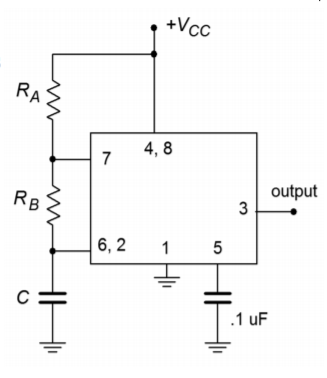
Figure \(\PageIndex{16}\): 555 astable connection.
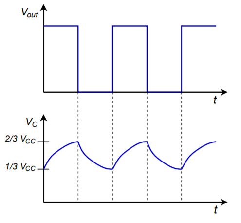
Figure \(\PageIndex{17}\): 555 astable waveforms.
The frequency of oscillation clearly depends only on C, RA, and RB. The time periods are
\[ T_{high} = 0.69(R_A+R_B)C \nonumber \]
\[ T_{low} = 0.69 R_B C \nonumber \]
This results in a frequency of
\[ f = \frac{1.44}{R_A +2 R_B} \nonumber \]
The duty cycle is normally defined as the high time divided by the period. The 555 documentation often reverses this definition, but we will stick with the industry norm.
\[ Duty Cycle = \frac{R_A+R_B}{R_A+2 R_B} \nonumber \]
A quick examination of the duty cycle Equation shows that there is no reasonable combination of resistors that will yield 50% duty cycle, let alone anything smaller. There is a simple trick to solve this problem, though. All you need to do is place a diode in parallel with RB as illustrated in Figure \(\PageIndex{18}\). The diode will be forward biased during the high time period and will effectively short out RB. During the low time period the diode will be reverse-biased, and RB will still be available for the discharge phase. If RA and RB are set to the same value, the end result will be 50% duty cycle. Of course, due to the non-ideal nature of the diode, this will not be perfect, so some adjustment of the resistor values may be in order. Further, note that if \(R_A\) is also replaced with a potentiometer (and perhaps a series limiting resistor) a
tunable square wave generator will result.
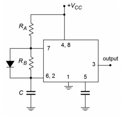
Figure \(\PageIndex{18}\): 555 with shunting diode for duty cycles \(\leq\) 50%.
Example \(\PageIndex{5}\)
Determine component values for a 2 kHz square wave generator with an 80% duty cycle. First, note the period is the reciprocal of the desired frequency, or 500 \(\mu\)s.
For an 80% duty cycle, that yields
\[ T_{high} = \text{ Duty Cycle } \times T \nonumber \]
\[ T_{high} = 0.8\times 500 \mu s \nonumber \]
\[ T_{high} = 400 \mu s \nonumber \]
\[ T_{low} = T−T_{high} \nonumber \]
\[ T_{low} = 500 \mu s−400 \mu s \nonumber \]
\[ T_{low} = 100 \mu s \nonumber \]
Choosing \(R_B = 10 k\Omega\),
\[ T_{low} = 0.69 R_B C \nonumber \]
\[ C = \frac{T_{low}}{0.69 R_B} \nonumber \]
\[ C = \frac{100 \mu s}{0.69\times 10 k\Omega} \nonumber \]
\[ C = 14.5 nF \nonumber \]
\[ T_{high} = 0.69(R_A+R_B)C \nonumber \]
\[ R_A = \frac{T_{high}}{0.69C} − R_B \nonumber \]
\[ R_A = \frac{400 \mu s}{0.69\times 14.5 nF} − 10 k\Omega \nonumber \]
\[ R_A = 30k\Omega \nonumber \]