
8.3: Linear Regulators
- Page ID
- 3595

If a regulator's control element operates in its linear region, the regulator is said to be a linear regulator. Most linear regulator ICs are series mode types. The main advantages of linear regulators are their ease of use and accuracy of control. Their main disadvantage is low efficiency.
A basic linear regulator is shown in Figure \(\PageIndex{1}\). The series control element is the transistor \(Q_1\). This component is most often referred to as a pass transistor, because it allows current to pass through to the load. The pass transistor is driven by the op amp. The pass transistor's job is to amplify the output current of the op amp. The op amp constantly monitors its two inputs. The noninverting input sees the Zener voltage of device \(D_1\). \(R_1\) is used to properly bias \(D_1\). The op amp's inverting input sees the voltage drop across \(R_3\). Note that \(R_2\) and \(R_3\) make up a voltage divider with \(V_{load}\) as the divider's source. Remembering the basics of negative feedback, recall that the op amp will produce enough current to keep its two inputs at approximately the same level, thus keeping \(V_{error}\) at zero. In other words, the voltage across \(R_3\) should be equal to the Zener potential. As long as the op amp has a high enough output current capability, this equality will be maintained. Note that the \(V_{BE}\) drop produced by \(Q_1\) is compensated for, as it is within the feedback loop. The difference between the filtered input signal and the final \(V_{load}\) is dropped across the collector/emitter of \(Q_1\).
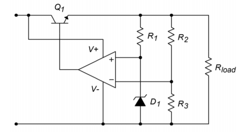
Figure \(\PageIndex{1}\): Basic op amp linear regulator.
In essence, the circuit of Figure \(\PageIndex{1}\) is a noninverting amplifier. \(V_{zener}\) is the input potential, and \(R_2\) and \(R_3\) take the place of resistors \(R_f\) and \(R_i\), respectively. \(V_{load}\) is found by using a variation of the basic gain formula:
\[ V_{load} = V_{zener} \frac{R_2+ R_3}{R_3} \label{8.3} \]
By choosing the appropriate ratios of resistors along with a suitable Zener, a wide range of output potentials may be achieved. Note that the op amp is fed from the nonregulated input. Any ripple that exists on this line will hardly affect the op amp's function. The ripple will be reduced by the op amp's PSRR (power supply rejection ratio). The Zener bias resistor, \(R_1\), is chosen so that it sets up a current that will guarantee Zener conduction. This is usually in the low milliamp range.
Example \(\PageIndex{1}\)
Determine the output of Figure \(\PageIndex{1}\) if \(R_1 = 5 k\Omega\), \(R_2 = 20 k\Omega\), \(R_3 = 10 k\Omega\) and \(V_{zener} = 3.9 V\). Assume that the filtered input is 20 V DC with no more than 3 V peak-to-peak ripple.
First, note that the input signal varies between a minimum of 18.5 V to a maximum of 21.5 V (20 V \(\pm\)1.5V peak). As long as the circuit doesn't try to produce more than the minimum input voltage and as long as all current and power dissipation limits are obeyed, everything should function correctly.
\[ V_{load} = V_{zener} \frac{R_2+ R_3}{R_3} \nonumber \]
\[ V_{load} = 3.9 V \times \frac{20 k+10 k}{10 k} \nonumber \]
\[ V_{load} = 11.7 V \nonumber \]
Due to the \(V_{BE}\) drop, the op amp needs to produce about 0.7 V more than this. Also, note that the Zener current may now be found.
\[ I_{zener} = \frac{V_{load} − V_{zener}}{R_1} \nonumber \]
\[ I_{zener} = \frac{11.7 V−3.9 V}{5 k} \nonumber \]
\[ I_{zener} = 1.56 mA \nonumber \]
This is a reasonable value.
Example \(\PageIndex{2}\)
Determine the power dissipation for \(Q_1\) and the circuit efficiency for Example \(\PageIndex{1}\) if the effective load resistance is 20 \(\Omega\).
First, \(I_{load}\) must be determined.
\[ I_{load} = \frac{V_{load}}{R_{load}} \nonumber \]
\[ I_{load} = \frac{11.7 V}{20} \nonumber \]
\[ I_{load} = 0.585A \nonumber \]
The dissipation of \(Q_1\) is the product of the current passing through it and the voltage across it. The current through \(Q_1\) is the load current. The voltage across \(Q_1\) is the difference between the filter's output and the load voltage. Because the filter's output contains a relatively small AC signal riding on DC, the average will equal the DC value, in this case, 20 V.
\[ V_{CE} = V_C − V_E \nonumber \]
\[ V_{CE} = 20 V − 11.7 V \nonumber \]
\[ V_{CE} = 8.3 V \nonumber \]
\[ P_D = I_C V_{CE} \nonumber \]
\[ P_D = 0.585 A\times 8.3 V \nonumber \]
\[ P_D = 4.86 W \nonumber \]
So, the pass transistor must dissipate 4.86 W and tolerate a current of 0.585 amps. The maximum collector-emitter voltage will occur at the peak input of 21.5 V. Therefore, the maximum differential is 9.8 V.
Finally, note that a 0.585 amp output would require a minimum \(\beta\) of
\[ \beta = \frac{I_C}{I_B} \nonumber \]
\[ \beta = \frac{585 mA}{20 mA} \nonumber \]
\[ \beta = 29.25 \nonumber \]
This assumes that the op amp can produce 20 mA and also ignores the small Zener and voltage divider currents at the output.
As far as efficiency is concerned, the input power and the load power need to be calculated. For load power,
\[ P_{load} = I_{load} V_{load} \nonumber \]
\[ P_{load} = .585 A\times 11.7 V \nonumber \]
\[ P_{load} = 6.844 W \nonumber \]
Ignoring the current requirements of the op amp, Zener and \(R_2/R_3\) divider, the supplied current equals 0.585 A. The average input voltage is 20 V.
\[ P_{in} = I_{in} V_{in} \nonumber \]
\[ P_{in} = 0.585 A\times 20 V \nonumber \]
\[ P_{in} = 11.7 W \nonumber \]
Efficiency, \(\eta \), is defined as the ratio of useful output to required input, so,
\[ \eta = \frac{P_{load}}{P_{in}} \nonumber \]
\[ \eta = \frac{6.844 W}{11.7 W} \nonumber \]
\[ \eta = 0.585 \ or \ 58.5 \% \nonumber \]
Therefore, 41.5% of the input power is wasted. In order to minimize the waste and maximize the efficiency, the input/output differential voltage needs to be as small as possible. For proper operation of the op amp and pass transistor, this usually means a differential lower than 2 to 3 V is impossible. Consequently, this form of regulation is very inefficient when the power supply must produce low output voltage levels.
Computer Simulation
A Multisim simulation of an op amp-based linear regulator, such as the one in Figure \(\PageIndex{1}\), is shown in Figure \(\PageIndex{2}\). The input signal is 20 V average, with a 120 Hz 2 V peak sine wave riding on it representing ripple. A 741 op amp is used as the comparison element along with a generic transistor for the pass device. The reference is a 5.2 V Zener diode. Given the circuit values, a manual calculation shows
\[ V_{out} = V_{zener} ( 1+ \frac{R_f}{R_i} ) \nonumber \]
\[ V_{out} = 5.2 V \times ( 1+ \frac{14k}{11k} ) \nonumber \]
\[ V_{out} = 11.8 V \nonumber \]
The output plot indicates a constant output at approximately 12.6 V. The discrepancy can be attributed to the non-ideal nature of the Zener diode (e.g., its internal resistance). Indeed, the initial solution indicates that the Zener potential (node 5) is approximately 5.5 V. A more accurate specification of the Zener diode (in particular, the BV and IBV parameters) would result in a much closer prediction. Another way of looking at this is to say that the 5.2 V Zener specification is too far below the actual Zener bias point for utmost accuracy (i.e., the manual calculation is somewhat sloppy and is, therefore, the one in error). This minor discrepancy aside, the time-domain plot does show the stability of the output signal in spite of the sizable input variations.
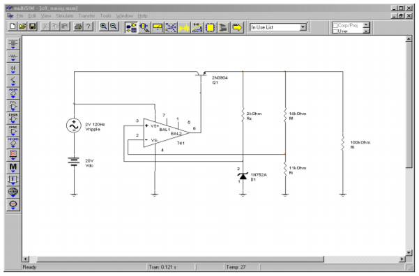
Figure \(\PageIndex{2a}\): Op amp regulator in Multisim.
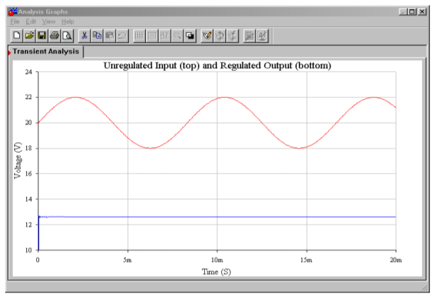
Figure \(\PageIndex{2b}\): Input and output waveforms from Multisim.
8.3.1: Three Terminal Devices
In an effort to make the designer's job ever easier, manufacturers provide circuits such as the one shown in Figure \(\PageIndex{1}\) in a single package. If you notice, the circuit really needs only three pins with which to connect to the outside world: input from the filter, ground, and output. These devices are commonly known as three pin regulators - hardly a creative name tag, but descriptive at least. Several different devices are available for varying current and power dissipation demands.
A typical “3 pin” device family is the LM340-XX/LM78XX and LM360- XX/LM79XX. The LM340-XX/LM78XX series is for positive outputs, while the LM360-XX/LM79XX series produces negative outputs. The “XX” indicates the rated load voltage. For example, the LM340-05 is a +5 V regulator, while the LM7912 is a -12 V unit. The most popular sizes are the 5, 12, and 15 V units. For simplicity, the series will be referred to as the LM78XX from here on.
A data sheet for the LM78XX series is shown in Figure \(\PageIndex{3}\). This regulator comes in several variants including TO-3, TO-220, and surface-mount versions. The TO-3 case version offers somewhat higher power dissipation capability. Output currents in excess of 1 A are available. As a side note, for lighter loads with lower current demands, the LM78LXX may be used. This regulator offers a 100 mA output and comes in a variety of packages.
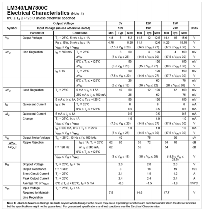
Figure \(\PageIndex{3a}\): LM78XX data sheet.
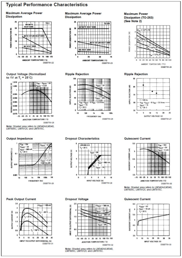
Figure \(\PageIndex{3b}\): LM78XX data sheet (continued). Reprinted courtesy of Texas Instrutments
The practical power dissipation limit of the LM78XX series, like any power device, is highly dependent on the type of heat sink used. The device graphs show that it can be as high as 20 W with the TO-3 case. The typical output voltage is within approximately 5 percent of the nominal value. This indicates the inherent accuracy of the IC, and is not a measure of its regulation abilities. Figures for both load and line regulation are given in the data sheet. For a variance in the line voltage of over 2:1, we can see that the output voltage varies by no more than 1 percent of the nominal output. Worst-case load regulation is just as good, showing no more than 1 percent deviation for a load current change from 5 mA up to 1.5 A. The regulator can also be seen to draw very little standby current, only 8.5 mA over a wide temperature range.
The output of the LM78XX series is fairly clean. The LM7815 shows an output noise voltage of 90 μV, typically, and an average ripple rejection of 70 dB. This means that ripple presented to the input of the regulator is reduced by 70 dB at the output. Because 70 dB translates to a factor of over 3000, this means that an input ripple signal of 1 V will be reduced to less than one-third of a millivolt at the output. It is worthwhile to note that this figure is frequency-dependent, as shown by the Ripple Rejection graph. Fortunately, the maximum value occurs in the desired range of 60 to 120 Hz.
The last major item in the data sheet is an extremely important one: Input Voltage Required To Maintain Line Regulation. This value is approximately 2.5 to 2.7 V greater than the nominal rating of the regulator. Without this headroom, the regulator will cease to function properly. Although it is desirable to keep the input/output differential voltage low in order to decrease device power dissipation and maximize efficiency, too low of a value will cripple the regulator. As seen in the Peak Output Current graph, the highest load currents are achieved when the differential is in the 5 to 10 V range.
In all cases, the devices offer thermal shutdown and output short-circuit protection. The maximum input voltage is limited to 35 V. Besides the LM78XX series, special high-current types with outputs in the 3 A and higher range are available.
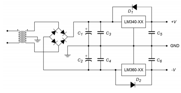
Figure \(\PageIndex{4}\): Dual supply for op amp circuits.
As an example, a bipolar power supply is shown in Figure \(\PageIndex{4}\). A center-tapped transformer is used to generate the required positive/negative polarities. \(C_1\) and \(C_2\) serve as the filter capacitors. The positive peak across each capacitor should not exceed 35 V, or the regulators may be damaged. The minimum voltage across the capacitors should be at least 3 V greater than the desired output level. The exact size of the capacitor depends on the amount of load current expected. In a similar manner, the magnitude of the load current will determine which case style will be used. Capacitors \(C_3\) and \(C_4\) are 220 nF units and are only required if the regulators are located several inches or more from the filter capacitors. If their use is required, \(C_3\) and \(C_4\) must be located very close the regulator. \(C_5\) and \(C_6\) are used to improve the transient response of the regulator. They are not used for filtering or for circuit stabilization. Through common misuse, \(C_5\) and \(C_6\) are often called “stability capacitors”, although this is not their function. Finally, diodes \(D_1\) and \(D_2\) protect the regulators from output over-voltage conditions, such as those experienced with inductive loads.
As you can see, designing moderate fixed voltage regulated power supplies with this template can be a very straightforward exercise. Once the basic power supply is configured, all that needs to be added are the regulators and a few capacitors and diodes. Quite simply, the regulator is “tacked on” to a basic capacitor-filtered unregulated supply. For a simple single polarity supply, the additional components can be reduced to a single regulator IC, the extra capacitors and diode being ignored.
8.3.2: Current Boosting
For very high output currents, it is possible to utilize external pass transistors to augment the basic linear regulator ICs. An example is shown in Figure \(\PageIndex{5}\). When the input current rises to a certain level, the voltage drop across \(R_1\) will be large enough to turn on transistor \(Q_1\). When \(Q_1\) starts to conduct, a current will flow through \(R_3\). As this current rises, the potential across \(R_3\) will increase to the point where the power transistor \(Q_2\) will turn on. \(Q_2\) will handle any further increases in load current. Normally, \(R_1\) is set so that the regulator is running at better than one-half of its maximum rating before switch over occurs. A typical value would be 22 \(\Omega\). For example, if switch over occurs at 1 A, the regulator will supply all of the load's demand up to 1 A. If the load requires more than 1 A, the regulator will supply 1 A, and the power transistor will supply the rest. Circuits of this type often need a minimum load current to function correctly. This “bleed-off” can be achieved by adding a single resistor in parallel with the load.
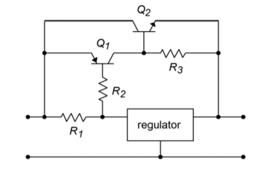
Figure \(\PageIndex{5}\): Pass transistors for increased load current.
Another possibility for increased output current is by paralleling devices and adding small ballast resistors. An example of this is shown in Figure \(\PageIndex{6}\). The ballast resistors are used to create local feedback. This reduces current hogging and forces the regulators to equally share the load current. (This is the same technique that is commonly used in high-power amplifiers so that multiple output transistors may be connected in parallel.) The size of the ballast resistors is rather low, usually 0.5 \(\Omega\) or less.
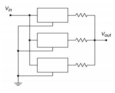
Figure \(\PageIndex{6}\): Parallel devices for increased load current
8.3.3: Low Dropout Regulators
Low dropout regulators (usually shortened to LDO) are a special subclass of ordinary linear regulators. Generally, they operate the same way, but with one major exception. Unlike normal linear regulators, LDOs do not require a large input-output differential voltage of several volts. Instead, LDOs will regulate with a differential as little as a few tenths of a volt. This minimum input-output differential is known as the dropout voltage. With a lowered headroom requirement, the LDO is much more efficient than the standard regulator, especially with low voltage outputs. An example is the LM2940. Like the LM78XX, this regulator is available at many popular output potentials, including 5, 12, and 15 V. It is rated for a 1 A output current. At maximum current, the dropout voltage is typically 0.5 V. At an output of 100 mA, the dropout voltage is typically 110 mV.
8.3.4: Programmable and Tracking Regulators
Along with the simple three-pin fixed regulators, a number of adjustable or programmable devices are available. Some devices also include features such as programmable current limiting. Also, it is possible to configure multiple regulators so that they track, or follow, each other.
One popular adjustable regulator is the LM317. This device is functionally similar to the 340 series discussed in the previous section. In essence, it has an internal reference of 1.25 V. By using an external voltage divider, a wide range of output potentials are available. The LM317 will produce a maximum current of 1.5 A and a maximum voltage of 37 V. A basic connection diagram is shown in Figure \(\PageIndex{7}\). The \(R_1/R_2\) divider sets the output voltage according to the formula
\[ V_{out} = 1.25 V( 1+ \frac{R_2}{R_1} ) + I_{adj} R_2 \nonumber \]
\(I_{adj}\) is the current flowing through the bottom adjust pin. \(I_{adj}\) is about 100 μA, and being this small, may be ignored to a first approximation. \(R_1\) is set to 240 \(\Omega\). D1 serves as a protection device for output over-voltages as seen in the preceding section. The 10 μF capacitor is used to increase the ripple rejection of the device. The addition of this capacitor will increase ripple rejection by at least 10 dB. Diode \(D_2\) is used to prevent possible destructive discharges from the 10 μF capacitor. In practice, \(R_2\) is set to a fixed size resistor for static supplies, or is a potentiometer for user-adjustable supplies.
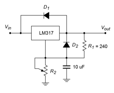
Figure \(\PageIndex{7}\): Basic LM317 regulator.
Example \(\PageIndex{3}\)
Determine a value for \(R_2\) so that the output is adjustable from a minimum of 1.25 V to a maximum of 15 V.
For the minimum value, \(R_2\) should be 0 \(\Omega\). Ignoring the effect of \(I_{adj}\), the maximum value is found by
\[ V_{out} = 1.25 V ( 1+ \frac{R_2}{R_1} ) \nonumber \]
\[ R_2 = R_1 \times ( \frac{V_{out}}{1.25 V} −1) \nonumber \]
\[ R_2 = 240 \times ( \frac{15 V}{1.25 V} −1) \nonumber \]
\[ R_2 = 2.64 k \nonumber \]
Normally, such a value is not available for stock potentiometers. A 2.5 k\(\Omega\) unit may be readily available, so \(R_1\) may be reduced a bit in order to compensate.
Computer Simulation
Figure \(\PageIndex{8}\) shows a simulation of the regulator designed in Example \(\PageIndex{3}\). The LM117 model used is very similar to the LM317. The maximum potentiometer value of 2.5 k\(\Omega\) is used here in order to see just how far off the design is from the 15 volt target. As in the earlier chapter simulation, a sine wave riding on a DC offset is used as the input to mimic the presence of ripple on the unregulated power source. The Transient Analysis of Multisim is used to plot the input and output waveforms. The circuit produces a very stable DC output as desired. Also, the level is only a few tenths of a volt shy of the desired 15 volt maximum, as expected. The simulation verifies the manual calculations quite well.
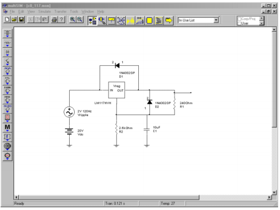
Figure \(\PageIndex{8a}\): LM317/LM117 simulation.
When using the LM317, if a minimum value greater than 1.25 V is needed, the pot may be placed in series with a fixed resistor. Alternately, precise preset values may be obtained through the use of a rotary switch and a bank of fixed resistors, as shown in Figure \(\PageIndex{9}\). As a matter of fact, these techniques may also be applied to the fixed three-pin devices presented in the previous section. For example, a LM7805 may be used as a 15 V regulator just by adding an external divider network as shown in Figure \(\PageIndex{10}\). You can think of the LM7805 as an LM317 with a 5 V reference. The exact values are not critical; what is important is that the ratio of the two resistors is 2:1.
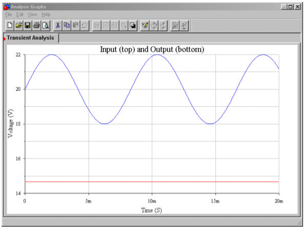
Figure \(\PageIndex{8b}\): Waveforms from Multisim.
One of the major problems with adjustable linear regulators is a “bottom end” limitation. It is easier for a regulator of this type to generate a high load current at a high load voltage than it is to generate a high load current at a low load voltage. The reason for this is that at low output voltages, the internal pass transistor sees a very high differential voltage. This results in very high power dissipation. If the device gets too hot, the thermal protection circuits may activate. From a user's standpoint, this means that the power supply may be able to produce a 15 V, 1 A output, but be unable to produce a 5 V, 1 A output.
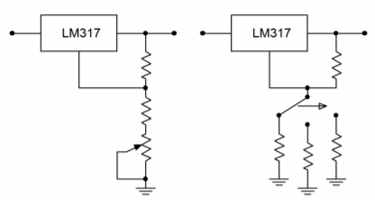
Figure \(\PageIndex{9}\): Adjustable regulation.
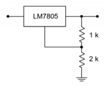
Figure \(\PageIndex{10}\): Varying output voltage with a fixed regulator.
Another popular regulator IC is the LM723. This device is of a more modular design and allows for preset current limiting. The equivalent circuit of 723 is shown in Figure \(\PageIndex{11}\). By itself, the LM723 is only capable of producing 150 mA. With the use of external pass transistors, an LM723-based regulator may produce several amps of load current. The internal reference is approximately 7.15 V. Because of this, two basic configurations exist: one for outputs below 7 V, and one for outputs above 7 V. These configurations and their output formulas are shown in Figure \(\PageIndex{12}\).
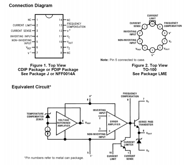
Figure \(\PageIndex{11}\): LM723 equivalent circuit. Reprinted courtesy of Texas Instrutments
By combining Figure \(\PageIndex{10}\) with Figure \(\PageIndex{11}\) and redrawing the results in Figures \(\PageIndex{13a}\) and \(\PageIndex{13b}\) you can see a strong resemblance to the basic op amp regulator encountered earlier. Figure \(\PageIndex{13a}\) is used for outputs greater than the 7.15 V reference. As such, resistors \(R_1\) and \(R_2\) are used to set the gain of the internal amplifier (i.e., the amount by which the reference will be multiplied). Resistor \(R_3\) simply serves as DC bias compensation for \(R_1\) and \(R_2\). For outputs less than the reference, \(R_1\) and \(R_2\) serve as a voltage divider, which effectively reduces the reference, whereas the amplifier operates with a gain of unity. Again, R3 serves as bias compensation. In short, the output voltage is once again determined by the reference voltage in conjunction with a pair of resistors. In both cases, the output current limit is set by
\[ I_{limit} = \frac{V_{sense}}{R_{sc}} \nonumber \]
Where \(V_{sense}\) is approximately 0.65 V at room temperature (for other temperatures, a \(V_{sense}\) graph is given in the LM723 data sheet). This Equation may be found on the manufacturer's data sheet, but may be readily derived by inspecting Figure \(\PageIndex{13}\). Resistor \(R_{sc}\) is placed in series with the load, and thus, the current through it is the load current (ignoring the small current required by the adjustment resistors). The current limit transistor is connected so that the voltage across \(R_{sc}\) is applied to this transistor's base-emitter junction. The collector of the current limit transistor is connected to the base of the output pass transistor. If the output current rises to the point where the voltage across \(R_{sc}\) exceeds approximately 0.65 V, the current limit transistor will turn on, thus shunting output drive current away from the output pass transistor. As you can see, the formula for \(I_{limit}\) is little more than the direct application of Ohm's Law. This scheme is similar to the method examined in Chapter Two to safely limit an op amp's output current.
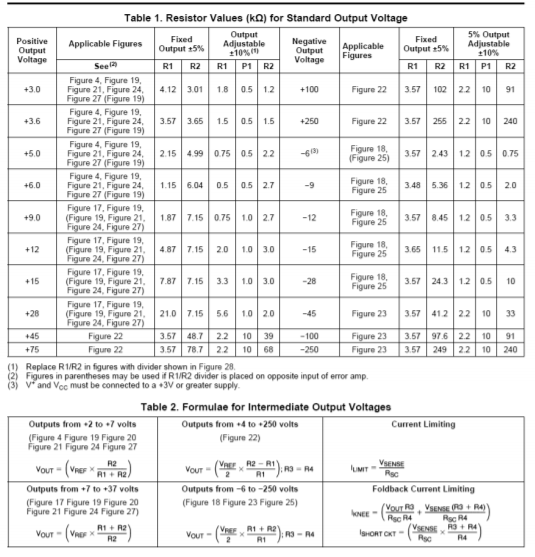
Figure \(\PageIndex{12}\): LM723 “hook ups”. Reprinted courtesy of Texas Instrutments
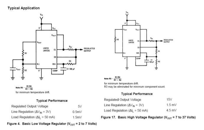
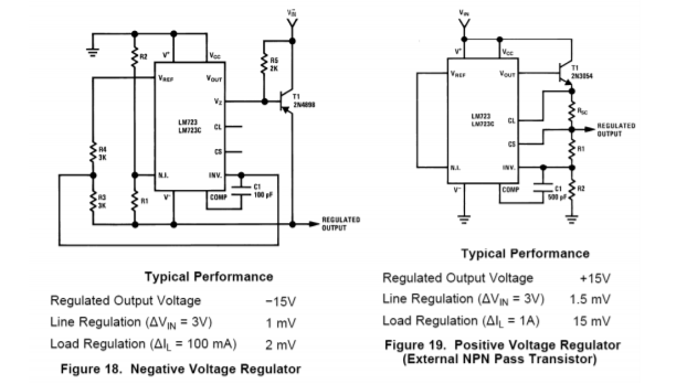
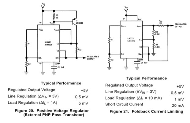
Figure \(\PageIndex{12}\) (continued): LM723 “hook ups”. Reprinted courtesy of Texas Instrutments
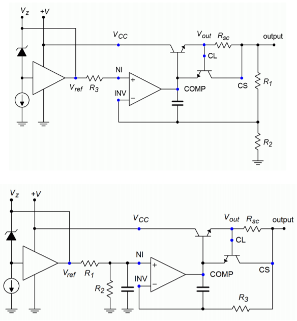
Figure \(\PageIndex{13}\): Two basic configurations of an LM723 regualtor. a. Output > 7.15 volts (top). b. Output < 7.15 volts (bottom).
Example \(\PageIndex{4}\)
Design a +12 V regulator using the LM723, with a current limit of 50 mA.
The basic form for this is the version shown in \(\PageIndex{12.2}\). The appropriate output Equation is
\[ V_{out} = V_{ref} \frac{R_1+R_2}{R_2} \nonumber \]
Choosing an arbitrary value for \(R_2\) of 10 k\(\Omega\), and then solving for \(R_1\),
\[ R_1 = \frac{V_{out}}{V_{ref}} R_2 − R_2 \nonumber \]
\[ R_1 = \frac{12V}{7.15 V} 10 k − 10 k \nonumber \]
\[ R_1 = 6.78 k \nonumber \]
For the current sense resistor,
\[ I_{limit} = \frac{V_{sense}}{R_{sc}} \nonumber \]
\[ R_{sc} = \frac{V_{sense}}{I_{limit}} \nonumber \]
\[ R_{sc} = \frac{0.65 V}{50 mA} \nonumber \]
\[ R_{sc} = 13 \Omega \nonumber \]
Finally, for minimum temperature drift, \(R_3\) is included, and set to \(R_1 || R_2\)
\[ R_3 = R_1 || R_2 \nonumber \]
\[ R_3 = 10 k || 6.78 k \nonumber \]
\[ R_3 = 4.04 k \nonumber \]
The completed circuit is shown in Figure \(\PageIndex{14}\).
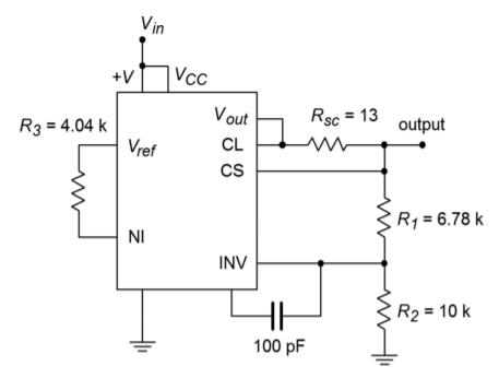
Figure \(\PageIndex{14}\): Completed 12 volt circuit for Example \(\PageIndex{4}\).
Example \(\PageIndex{5}\)
Using the LM723, design a continuously adjustable 2V to 5V supply, with a current limit of 1.0 A.
The basic form for this is the version shown in Figure \(\PageIndex{12.1}\). The appropriate output Equation is
\[ V_{out} = V_{ref} \frac{R_2}{R_1+R_2} \nonumber \]
We need to make a few modifications to the basic form in order to accommodate the high output current and the output voltage adjustment. One possibility is shown in Figure \(\PageIndex{15}\).
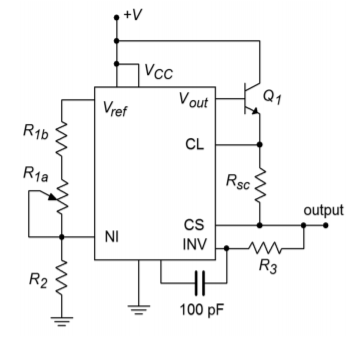
Figure \(\PageIndex{15}\): Circuit for Example \(\PageIndex{5}\): 2 V to 5 V regulator, 1 amp.
In order to produce a 1 A load current, an external pass transistor will be used. To obtain the desired voltage adjustment, resistor \(R_1\) is replaced with a series potentiometer/resistor combination (\(R_{1a}, R_{1b}\)). In this fashion, the minimum value for R1 will be R1b, and the maximum value will be \(R_{1a} + R_{1b}\). There are several ways in which we can approach the calculation of these three resistors. Perhaps the easiest is to pick a value for \(R_2\) and then determine values for \(R_{1a}\) and \(R_{1b}\). Though this is fairly straightforward, it is not very practical because you will most likely wind up with an odd size for the potentiometer. A better, though admittedly more involved, approach revolves around the selection of a reasonable pot value, such as 10 k\(\Omega\). Given the desired output potentials, the other two resistors may be found.
First of all, note that these three resistors are nothing more than a voltage divider. The output voltage Equation may be rewritten as
\[ \frac{R_1+R_2}{R_2} = \frac{V_{ref}}{V_{out}} \nonumber \]
For the maximum case, we have
\[ \frac{R_{1b} + R_2}{R_2} = \frac{V_{ref}}{V_{out}} \nonumber \]
\[ \frac{R_{1b} + R_2}{R_2} = \frac{7.15 V}{5 V} \nonumber \]
\[ \frac{R_{1b} + R_2}{R_2} = 1.43 \nonumber \]
If we consider \(R_2\) to be unity, we may say that the ratio of the two resistors to \(R_2\) is 1.43:1, or, that the ratio of \(R_{1b}\) to \(R_2\) is 0.43:1.
For the minimum case, we have
\[ \frac{R_{1a} + R_{1b} + R_2}{R_2} = \frac{V_{ref}}{V_{out}} \nonumber \]
\[ \frac{R_{1a} + R_{1b} + R_2}{R_2} = \frac{7.15 V}{2 V} \nonumber \]
\[ \frac{R_{1a} + R_{1b} + R_2}{R_2} = 3.575 \nonumber \]
We may say that the ratio of the three resistors to \(R_2\) is 3.575:1, or that the ratio of \(R_{1a}+R_{1b}\) to \(R_2\) is 2.575:1. Because we already know that the ratio of \(R_{1b}\) to \(R_2\) is 0.43:1, the ratio of \(R_{1a}\) to \(R_2\) must be the difference, or 2.145:1. Because we chose 10 k\(\Omega\) for \(R_{1a}\),
\[ R_2 = \frac{R_{1a}}{2.145} \nonumber \]
\[ R_2 = \frac{10 k}{2.145} \nonumber \]
\[ R_2 = 4.66 k \nonumber \]
Similarly,
\[ R_{1b} = R_2\times 0.43 \nonumber \]
\[ R_{1b} = 4.66k\times 0.43 \nonumber \]
\[ R_{1b} = 2k \nonumber \]
For the current sense resistor,
\[ I_{limit} = \frac{V_{sense}}{R_{sc}} \nonumber \]
\[ R_{sc} = \frac{V_{sense}}{I_{limit}} \nonumber \]
\[ R_{sc} = \frac{0.65V}{1.0 A} \nonumber \]
\[ R_{sc} = 0.65 \Omega \nonumber \]
For minimum temperature drift, \(R_3\) is included, and set to \(R_1 || R_2\). Because \(R_1\) is adjustable, a midpoint value will be used.
\[ R_3 = R_1 || R_2 \nonumber \]
\[ R_3 = 6k || 4.66k \nonumber \]
\[ R_3 = 2.62 k \nonumber \]
The final calculation involves the external pass transistor. This design uses a 1 A output, so this device must be able to handle this current continuously. Also, a minimum \(\beta\) specification is required. As the LM723 will be driving the pass transistor, the LM723 only needs to produce base drive current. With a maximum output of 150 mA, this translates to a minimum \(\beta\) of
\[ \beta_{min} = \frac{I_c}{I_b} \nonumber \]
\[ \beta_{min} = \frac{1 A}{150 mA} \nonumber \]
\[ \beta_{min} = 6.67 \nonumber \]
This value should pose no problem for a power transistor.
Besides the applications we have just examined, the LM723 can also be used to make negative regulators, switching regulators, and other types as well. One useful variation on the basic theme is the use of foldback current limiting, as seen in Figure \(\PageIndex{12.6}\). Unlike the ordinary form of current limiting, foldback limiting actually produces a decrease in output current once the limit point is reached. Figure \(\PageIndex{16a}\) shows the effect of ordinary limiting. Once the limit point is reached, further demands by the load will be ignored. The problem with this arrangement is that under short circuit conditions, the pass transistor will be under heavy stress. Because the load is shorted, so \(V_{load}\) = 0, and therefore, a large potential will drop across the pass transistor. This device is already handling the full current draw, thus the resulting power dissipation can be very high. Foldback limiting gets around this problem by lowering the output current as the pass transistor's voltage increases. Note how in Figure \(\PageIndex{16b}\), the current limit curve does not drop straight down to the limit point, but rather, as the load demand increases, the current drops back to \(I_{sc}\). By limiting the current in this fashion, a much lower power dissipation is achieved.
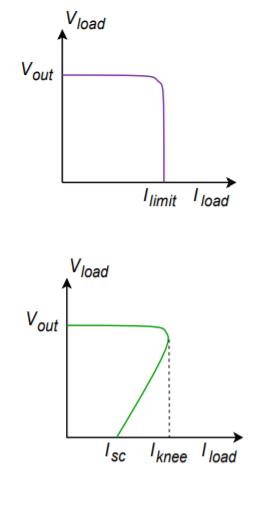
Figure \(\PageIndex{16}\): Current limiting. a. Ordinary (top). b. Fold back (bottom).
Our last item of interest in this section is the LT3032 dual regulator series. These devices are of particular interest to the op amp technician and designer. The LT3032 is available as a fixed bipolar regulator at outputs of \(\pm\)3.3, \(\pm\)5, \(\pm\)12 or \(\pm\)15 volts. Another variant offers adjustable output from \(\pm\)1.22 volts up to \(\pm\)20 volts. Output current capability is up to 150 mA. These devices are ideal for powering general purpose op amp circuits.
The circuit in Figure \(\PageIndex{17}\) is a minimum parts-configuration dual regulator requiring only two resistors and a capacitor per side.. All that is needed ahead of this circuit is a standard transformer, rectifier and filter capacitor arrangement, such as that found in Figure \(\PageIndex{4}\). The maximum output (unloaded) of the filter capacitors should be no more than 20 V in order to prevent damage to the LT3032. This circuit is certainly simpler than the LM317-based regulator of Figure \(\PageIndex{7}\), and not much different from an LM340-based design. In fact, note the similarity of the design equations presented for the LM317 and the LT3032. Again, we see that the output potential is found essentially by multiplying a reference voltage by a series-parallel voltage gain. The downside is that its power dissipation and maximum currents are considerably lower than its LM340 or LM317 counterparts. Still, a 150 mA output capability is sufficient to drive a large number of op amps and other small signal devices.
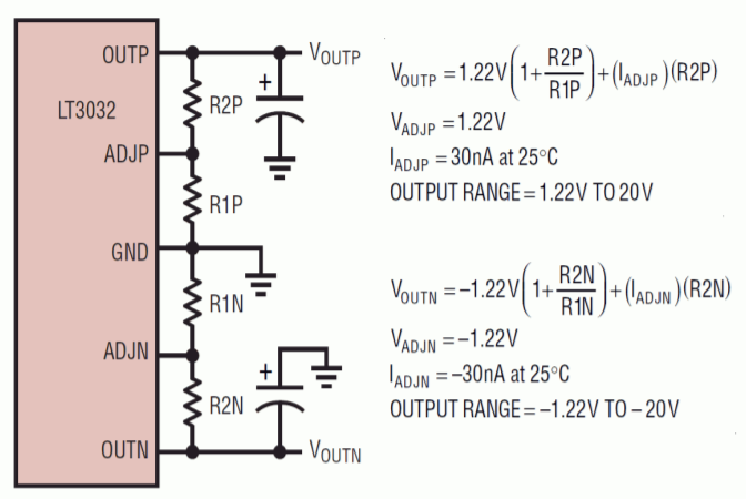
Figure \(\PageIndex{17}\): LT3032 pinout and formulas. Reprinted with permission of Linear Technology
Current limiting and thermal shutdown are built-in. Other design features include the fact that the LT3032 is a low drop-out regulator requiring only a 300 millivolt differential per channel. ESD (electrostatic discharge) protection is included and reverse output polarity protection diodes are not required. Further, the addition of a small 10 nF capacitor at each output will reduce regulator noise voltage down to the 20 to 30 microvolt RMS range.
There are many other linear regulator ICs available to the designer than have been presented here. Many of these devices are rather specialized, and all units seem to have their own special set of operational formulas and graphs. There are, however, a few common threads among them all. First, due to the relative internal complexity, manufacturers often give very specific application guidelines for their particular ICs. The resulting design sequence is rather like following a cookbook and makes the designer's life much easier. Second, as mentioned at the outset, all linear regulators tend to be rather inefficient. This inefficiency is inherent in the design and implementation of the linear regulation circuits, and cannot be avoided. At best, the inefficiency can be minimized for a given application. In order to achieve high efficiency, a different topology must be considered. One alternative is the switching regulator.