
2.4: Generalized Scattering Parameters
- Page ID
- 41092
The scattering parameters up to now are known as normalized \(S\) parameters because they have the same reference impedance at each port. However the qualification ‘normalized’ is not used unless it is necessary to distinguish them from a more general form of \(S\) parameters. In this section generalized \(S\) parameters that have different reference impedances at each of the ports are considered. These are particularly useful in designing amplifiers but are also useful in measurements where the system impedance of a design may not be the same as the reference impedance of the measurement system. For example an RFIC may have a system impedance of \(100\:\Omega\), but the measurement system have a reference impedance of \(50\:\Omega\).
2.4.1 The \(N\)-Port Network
The \(N\)-port network is a generalization of a two-port, as you may have guessed. A network with many ports is shown in Figure 2.3.10. Again, each port consists of a pair of terminals, one of which is the reference for voltage. Each port has equal and opposite currents at the two terminals. The incident and reflected voltages at any port can be related to each other using the voltage scattering parameter matrix relation:
\[\label{eq:1}\left[\begin{array}{c}{V_{1}^{-}}\\{V_{2}^{-}}\\{\vdots}\\{V_{N}^{-}}\end{array}\right]=\left[\begin{array}{cccc}{S_{11}}&{S_{12}}&{\cdots}&{S_{1N}} \\ {S_{21}}&{S_{22}}&{\cdots}&{S_{2N}} \\ {\vdots}&{}&{\ddots}&{}\\{S_{N1}}&{S_{N2}}&{\cdots}&{S_{NN}}\end{array}\right]=\left[\begin{array}{c}{V_{1}^{+}}\\{V_{2}^{+}}\\{\vdots}\\{V_{N}^{+}}\end{array}\right] \]
or in compact form as
\[\label{eq:2}\mathbf{V}^{-}=\mathbf{SV}^{+} \]
Notice that
\[\label{eq:3}S_{ij}=\left.\frac{V_{i}^{-}}{V_{j}^{+}}\right|_{V_{k}^{+}=0\text{ for }k\neq j} \]
In words, \(S_{ij}\) is found by driving Port \(j\) with an incident wave of voltage \(V_{j}^{+}\) and measuring the reflected wave \(V_{i}^{−}\) at Port \(i\), with all ports other than \(j\) terminated in a matched load. Reflection and transmission coefficients can also be defined using the above relationship, provided that the ports are terminated in matched loads:
- \(S_{ii}\): reflection coefficient seen looking into Port \(i\)
- \(S_{ij}\): transmission coefficient from \(j\) to \(i\).
2.4.2 Power Waves
The \(S\) parameters used so far have the same reference impedance at each port. These can be generalized so that the reference impedances at each port can be different. These are useful if the actual system being considered has different loading conditions at the ports. Generalized \(S\) parameters, denoted here as \(^{G}S\), are defined in terms of what are called root power waves, which in turn are defined using forward- and backward-traveling voltage waves. Consider the \(N\)-port network of Figure 2.3.10, where the \(n\)th port has a reference transmission line of characteristic impedance \(Z_{0n}\), which can have infinitesimal length. The transmission line at the \(n\)th port serves to separate the forward- and backward-traveling voltage (\(V_{n}^{+}\) and \(V_{n}^{−}\)) and current (\(I_{n}^{+}\) and \(I_{n}^{−}\)) waves.
The reference characteristic impedance matrix \(\mathbf{Z}_{0}\) is a diagonal matrix, \(\mathbf{Z}_{0} = \text{diag}(Z_{01}\ldots Z_{0n}\ldots Z_{0N})\), and the root power waves at the \(n\)th port, \(a_{n}\) and \(b_{n}\), are defined by
\[\label{eq:4}a_{n}=V_{n}^{+}/\sqrt{\Re\{Z_{0n}\}}\quad\text{and}\quad b_{n}=V_{n}^{-}\sqrt{\Re\{Z_{0n}\}} \]
and shown in Figure \(\PageIndex{1}\) and are often called just power waves. The unit of the \(a\) and \(b\) values is root power, that is, in the SI unit system, \(\sqrt{\text{W}}\). In matrix form
\[\begin{align}\label{eq:5}\mathbf{a}&=\mathbf{Z}_{0}^{-1/2}\mathbf{V}^{+}=\mathbf{Y}_{0}^{1/2}\mathbf{V}^{+} &\mathbf{b}&=\mathbf{Z}_{0}^{-1/2}\mathbf{V}^{-}=\mathbf{Y}_{0}^{1/2}\mathbf{V}^{-} \\ \label{eq:6}\mathbf{V}^{+}&=\mathbf{Z}_{0}^{1/2}\mathbf{a}=\mathbf{Y}_{0}^{-1/2}\mathbf{a} &\mathbf{V}^{-}&=\mathbf{Z}_{0}^{1/2}\mathbf{b}=\mathbf{Y}_{0}^{-1/2}\mathbf{b}\end{align} \]
where
\[\begin{align}\label{eq:7}\mathbf{a}&=[a_{1}\ldots a_{n}\ldots a_{N}]^{\text{T}} &\mathbf{b}&=[b_{1}\ldots b_{n}\ldots b_{N}]^{\text{T}} \\ \label{eq:8}\mathbf{V}^{+}&=[V_{1}^{+}\ldots V_{n}^{+}\ldots V_{N}^{+}]^{\text{T}} &\mathbf{V}^{-}&=[V_{1}^{-}\ldots V_{n}^{-}\ldots V_{N}^{-}]^{\text{T}}\end{align} \]
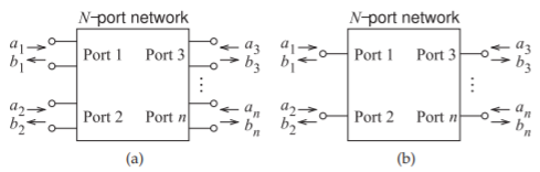
Figure \(\PageIndex{1}\): \(N\)-ports defining the \(a\) and \(b\) root power waves: (a) two-terminal ports; and (b) ports on their own.
and the characteristic admittance matrix is \(\mathbf{Y}_{0} =\mathbf{Z}_{0}^{−1}\). The power waves are interpreted as describing power flow:
\[\frac{1}{\sqrt{2}}|a_{n}|=\sqrt{\text{incident power at Port }n}\nonumber \]
and
\[\label{eq:9}\frac{1}{\sqrt{2}}|b_{n}|=\sqrt{\text{power leaving at Port }n} \]
That is, for example, the incident (or available) power at Port \(n\), referenced to \(Z_{0n}\), is \(\frac{1}{2}|a_{n}|^{2}\) and the reflected power at the port is \(\frac{1}{2}|b_{n}|^{2}\). Thus the power delivered by the \(n\)th port is \(\frac{1}{2}(|b_{n}|^{2} − |a_{n}|^{2})\).
After some manipulation it can be shown that on each reference line the power waves can be related to the total voltages and currents as
\[\label{eq:10}\mathbf{a}=\frac{\mathbf{V}+\mathbf{Z}_{0}\mathbf{I}}{2\sqrt{\Re\{\mathbf{Z}_{0}\}}}\quad\text{and}\quad\mathbf{b}=\frac{\mathbf{V}-\mathbf{Z}_{0}^{\ast}\mathbf{I}}{2\sqrt{\Re\{\mathbf{Z}_{0}\}}} \]
where \(\mathbf{V}\) and \(\mathbf{I}\) are vectors of total voltage and total current. Now, generalized \(S\) parameters can be formally defined as
\[\label{eq:11}\mathbf{b}=\:^{G}\mathbf{Sa} \]
thus \(\mathbf{Y}_{0}^{1/2}\mathbf{V}^{−} =\:^{G}\mathbf{SY}_{0}^{1/2}\mathbf{V}^{+}\), and so \(\mathbf{V}^{−} = \mathbf{Y}_{0}^{−1/2}\:^{G}\mathbf{SY}_{0}^{1/2}\mathbf{V}^{+}\). This reduces to \(\mathbf{V}^{−} =\:^{G}\mathbf{SV}^{+}\) when all of the reference transmission lines have the same characteristic impedance. However, when the ports have different reference impedances, \(\mathbf{S}^{V}\) is used for voltage scattering parameters and \(\mathbf{S}^{I}\) for current scattering parameters, where \(\mathbf{V}^{−}= \mathbf{S}^{V}\mathbf{V}^{+}\) and \(\mathbf{I}^{−}= \mathbf{S}^{I}\mathbf{I}^{+}\).
The following conversion relationships can also be derived:
\[\begin{align}\label{eq:12}\mathbf{S}^{I}&=\Re\{\mathbf{Z}_{0}\}^{-\frac{1}{2}G}\mathbf{S}\Re\{\mathbf{Z}_{0}\}^{\frac{1}{2}} \\ \label{eq:13} \mathbf{S}^{V}&=\mathbf{Z}_{0}\Re\{\mathbf{Z}_{0}\}^{-\frac{1}{2}G}\mathbf{S}\Re\{\mathbf{Z}_{0}\}^{\frac{1}{2}}\{\mathbf{Z}_{0}^{\ast}\}^{-1}\end{align} \]
where \(\Re\{\mathbf{Z}_{0}\}^{\frac{1}{2}}=\text{diag}\{\sqrt{\Re\{Z_{01}\}},\:\sqrt{\Re\{Z_{02}\}},\ldots\sqrt{\Re\{Z_{0n}\}}\}\).
Recall that \(^{G}\mathbf{S}\) is in terms of \(\mathbf{a}\) and \(\mathbf{b}\), \(\mathbf{S}^{\mathbf{I}}\) is in terms of \(\mathbf{I}^{−}\) and \(\mathbf{I}^{+}\), and \(\mathbf{S}^{\mathbf{V}}\) is in terms of \(\mathbf{V}^{−}\) and \(\mathbf{V}^{+}\). When port impedances and reference resistances are real, Equations \(\eqref{eq:12}\) and \(\eqref{eq:13}\) assume the simpler forms
\[\begin{align}\label{eq:14}\mathbf{S}^{I}&=-\mathbf{R}_{0}^{-\frac{1}{2}}\:^{G}\mathbf{S}\mathbf{R}_{0}^{\frac{1}{2}}=-\:^{G}\mathbf{S} \\ \label{eq:15}\mathbf{S}^{\mathbf{V}}&=\mathbf{R}_{0}\mathbf{R}_{0}^{-\frac{1}{2}}\:^{G}\mathbf{S}\mathbf{R}_{0}^{\frac{1}{2}}\mathbf{R}_{0}^{\ast^{-1}}=\mathbf{R}_{0}(\mathbf{R}_{0}^{\ast})^{-1}\:^{G}\mathbf{S}=^{G}\mathbf{S}\end{align} \]
where \(\mathbf{R}_{0}^{\frac{1}{2}}=\text{diag}\{\sqrt{R_{01}},\:\sqrt{R_{02}},\ldots ,\sqrt{R_{0n}}\}\), with \(R_{0n}\) being the reference resistance at the nth port. In addition, if the reference resistances at each port are the same, all of the various scattering parameter definitions become equivalent (i.e., \(\mathbf{S}^{\mathbf{V}} = −\mathbf{S}^{\mathbf{I}} =\:^{G}\mathbf{S} = \mathbf{S}\)), where \(\mathbf{S}\) is the normalized \(S\) parameter matrix, also called the normalized \(S\) parameter matrix.
The reciprocity condition for generalized \(S\) parameters is \(^{G}S_{12} =\:^{G}S_{21}Z_{01}/Z_{02}\).
Example \(\PageIndex{1}\): Generalized Scattering Parameters of a Through Connection
Develop the generalized scattering parameters of a through connection with a reference impedance \(Z_{01}\) at Port \(\mathsf{1}\) and a reference impedance \(Z_{02}\) at Port \(\mathsf{2}\).
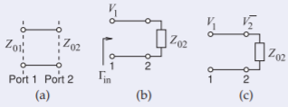
Figure \(\PageIndex{2}\)
Solution
The through connection is shown in (a) and in (b) is the configuration to determine \(S_{11}\) as \(V_{2}^{+}=0= a_{2}\) since Port \(\mathsf{2}\) is terminated in \(Z_{02}\). Then
\[\label{eq:16}^{G}S_{11}=\Gamma_{\text{in}}=\frac{Z_{02}-Z_{01}}{Z_{02}+Z_{01}}\quad\text{and similarly}\quad ^{G}S_{22}=\frac{Z_{01}-Z_{02}}{Z_{02}+Z_{01}}=-\:^{G}S_{11} \]
Figure (b) is used to determine \(S_{21}\) as here \(V_{2}^{+}=0= a_{2}\)
\[\label{eq:17}V_{2}^{-}=b_{2}\sqrt{\Re\{Z_{02}\}}=V_{1}=V_{1}^{+}+V_{1}^{-}=V_{1}^{+}(1+S_{11})=a_{1}\sqrt{\Re\{Z_{01}\}} \]
Thus,
\[\label{eq:18}^{G}S_{21}=\left.\frac{b_{2}}{a_{1}}\right|_{a_{2}=0}=\frac{\sqrt{\Re\{Z_{01}\}}}{\sqrt{\Re\{Z_{02}\}}}(1+\:^{G}S_{11})\quad\text{and also}\quad ^{G}S_{12}=\frac{\sqrt{\Re\{Z_{02}\}}}{\sqrt{\Re\{Z_{01}\}}}(1+\:^{G}S_{22}) \]
The generalized scattering parameter matrix of the through is
\[\label{eq:19}^{G}\mathbf{S}=\frac{1}{Z_{01}+Z_{02}}\left[\begin{array}{cc}{Z_{02}-Z_{01}}&{2Z_{01}\sqrt{\Re\{Z_{02}\}/\Re\{Z_{01}\}}}\\{2Z_{02}\sqrt{\Re\{_{01}\}/\Re\{Z_{02}\}}}&{Z_{01}-Z_{02}}\end{array}\right] \]
and for real \(Z_{01}\) and \(Z_{02}\)
\[\label{eq:20}^{G}\mathbf{S}=\frac{1}{Z_{01}+Z_{02}}\left[\begin{array}{cc}{Z_{02}-Z_{01}}&{2\sqrt{Z_{01}Z_{02}}}\\{2\sqrt{Z_{01}Z_{02}}}&{Z_{01}-Z_{02}}\end{array}\right] \]
For normalized \(S\) parameters the reference impedances at the ports are the same, i.e. \(Z_{01} = Z_{0} = Z_{02}\), and the normalized \(S\) parameters of the through are (as expected)
\[\label{eq:21}\mathbf{S}=\:^{N}\mathbf{S}=\left[\begin{array}{cc}{0}&{1}\\{1}&{0}\end{array}\right] \]
2.4.3 Scattering Parameters in Terms of \(a\) and \(b\) waves
Previously \(S\) parameters were defined in terms of forward- and backward-traveling voltage waves, see Section 2.3.3 and Equation (2.3.15). That definition is adequate if only one reference impedance is used throughout. A more general form of \(S\) parameters uses the \(a\) and \(b\) root power waves. This is still valid if only one reference impedance is used but they can also be used when the ports have different reference impedances. This more general definition for a two-port network, with respect to Figure \(\PageIndex{3}\), is
\[\label{eq:22}\left[\begin{array}{c}{b_{1}}\\{b_{2}}\end{array}\right]=\left[\begin{array}{cc}{S_{11}}&{S_{12}}\\{S_{21}}&{S_{22}}\end{array}\right]\left[\begin{array}{c}{a_{1}}\\{a_{2}}\end{array}\right] \]
Even if the reference impedances at ports \(\mathsf{1}\) and \(\mathsf{2}\) are the different. If the references impedance are the same and real, the usual case, the scattering parameters are identical when used to relate traveling voltage waves as in the following:
\[\label{eq:23}\left[\begin{array}{c}{V_{1}^{-}}\\{V_{2}^{-}}\end{array}\right]=\left[\begin{array}{cc}{S_{11}}&{S_{12}}\\{S_{21}}&{S_{22}}\end{array}\right]\left[\begin{array}{c}{V_{1}^{+}}\\{V_{2}^{+}}\end{array}\right] \]
2.4.4 Normalized and Generalized \(S\) Parameters
\(S\) parameters measured with respect to a common reference resistance are referred to as normalized \(S\) parameters. In almost all cases, measured \(S\) parameters are normalized to \(50\:\Omega\), as \(50\:\Omega\) cables and components are used in measurement systems. In other words, \(Z_{01} = Z_{02} =\ldots= Z_{0N} = R_{0} (= 50\:\Omega)\). Generalized \(S\) parameters can be used to simplify the design process of devices such as amplifiers. For example, it is often convenient to use the input and output impedances of an amplifier as the normalization impedances. Also, it is often desirable to be able to convert between measured \(S\) parameters (normalized to \(50\:\Omega\)) and generalized \(S\) parameters. Let \(^{N}\mathbf{S}\) be the measured (normalized) \(S\) parameter matrix. (So \(^{N}\mathbf{S}\) is the conventional \(S\) parameter matrix.) The development is tedious, but it can be shown that the generalized \(S\) parameters are
\[\label{eq:24}^{G}\mathbf{S}=(\mathbf{D}^{\ast})^{-1}(\:^{N}\mathbf{S}-\mathbf{Γ}^{\ast})(\mathbf{U}-\mathbf{Γ}\:^{N}\mathbf{S})^{-1}\mathbf{D} \]
where \(\mathbf{U}\) is the unit matrix \((\mathbf{U} = \text{diag}(1, 1,..., 1))\), \(R_{0}\) is the reference impedance of the normalized \(S\) parameters, \(^{N}\mathbf{S}\), and \(\mathbf{D}\) is a diagonal matrix with elements
\[\begin{align}\label{eq:25}D_{ii}&=|1-\Gamma_{i}^{\ast}|^{-1}(1-\Gamma_{i})\sqrt{1-|\Gamma_{i}|^{2}} \\ \label{eq:26}\Gamma_{i}&=(Z_{0i}-R_{0})(Z_{0i}+R_{0})^{-1}\quad i=1,2,\ldots ,N\end{align} \]
and \(\mathbf{Γ}\) is a diagonal matrix with elements \(\Gamma_{i}\). \(Z_{0i}\) is the system impedance at Port \(i\) to which the generalized \(S\) parameters are to be referred.
2.4.5 Change of Reference Impedance
The result in the section above can be used to change scattering parameters referenced to a real impedance \(R_{1}\) (i.e., \(^{R1}\mathbf{S}\)) to scattering parameters referenced to \(R_{2}\) (i.e., \(^{R2}\mathbf{S}\)). Note that \(^{R1}\mathbf{S}\) and \(^{R2}\mathbf{S}\) are the conventional or normalized \(S\) parameters. The elements in Equations \(\eqref{eq:25}\) and \(\eqref{eq:26}\) become
\[\begin{align}\label{eq:27}D_{ii}&=D=|1-\Gamma_{R2}|^{-1}(1-\Gamma_{R2})\sqrt{1-|\Gamma_{R2}|^{2}}=\sqrt{1-|\Gamma_{R2}|^{2}} \\ \label{eq:28}\Gamma_{R2}&=(R_{2}-R_{1})(R_{2}+R_{1})^{-1}\end{align} \]
and \(|\Gamma_{R2}| < 1\). So Equation \(\eqref{eq:24}\) becomes
\[\label{eq:29}^{R2}\mathbf{S}=\mathbf{D}^{-1}(\:^{R1}\mathbf{S}-\mathbf{Γ})(\mathbf{U}-\mathbf{Γ}^{R1}\:\mathbf{S})^{-1}\mathbf{D}=(\:^{R1}\mathbf{S}-\mathbf{Γ})(\mathbf{U}-\mathbf{Γ}^{R1}\:\mathbf{S})^{-1} \]
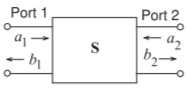
Figure \(\PageIndex{3}\): Definition of \(S\) parameters in terms of \(a\) and \(b\) root power waves. \(a_{1} = V_{1}^{+}/\Re\{Z_{01}\},\: b_{1} = V_{1}^{−}/\Re\{Z_{01}\},\: a_{2} = V_{2}^{+}/\Re\{Z_{02}\},\: b_{2} = V_{2}^{−}/\Re\{Z_{02}\}\). Incident power at Port \(\mathsf{1}\) (2) is \(|a_{1}|^{2} (|a_{2}^{2})\). Power leaving Port \(\mathsf{1}\) (2) is \(|b_{1}|^{2} (|b_{2}^{2})\)
since \(\mathbf{D}\) is a diagonal matrix with all diagonal entries the same. So for a two-port
\[\begin{align} ^{R2}\mathbf{S}&=\left[\begin{array}{cc}{^{R2}S_{11}}&{^{R2}S_{12}} \\ {^{R2}S_{21}}&{^{R2}S_{22}}\end{array}\right] \nonumber \\ \label{eq:30}&=\left[\begin{array}{cc}{^{R1}S_{11}-\Gamma_{R2}}&{^{R1}S_{12}} \\ {^{R1}S_{21}}&{^{R1}S_{22}-\Gamma_{R2}}\end{array}\right] \left[\begin{array}{cc}{1-\Gamma_{R2}\:^{R1}S_{11}}&{-\Gamma_{R2}\:^{R1}S_{12}} \\ {-\Gamma_{R2}\:^{R1}S_{21}}&{1-\Gamma_{R2}\:^{R1}S_{22}}\end{array}\right] ^{-1} \end{align} \]
Example \(\PageIndex{2}\): Change of Reference Impedance
An attenuator has the \(50\:\Omega\: S\) parameters:
\[\label{eq:31}^{50}\mathbf{S}=\left[\begin{array}{cc}{0}&{0.3162} \\ {0.3162}&{0}\end{array}\right] \]
What are the \(S\) parameters referenced to \(75\:\Omega\)?
Solution
The conversion uses Equation \(\eqref{eq:30}\) with \(R_{1} = 50\:\Omega\) and \(R_{2} = 75\:\Omega\). So \(\Gamma_{75} = (75 − 50)/(75 + 50) = 0.2\). Thus the \(S\) parameters referenced to \(75\:\Omega\) are
\[\begin{align} ^{75}\mathbf{S}&=\left[\begin{array}{cc}{^{50}S_{11}-\Gamma_{75}}&{^{50}S_{12}} \\ {^{50}S_{21}}&{^{50}S_{22}-\Gamma_{75}}\end{array}\right] \left[\begin{array}{cc}{1-\Gamma_{75}\:^{50}S_{11}}&{-\Gamma_{75}\:^{50}S_{12}} \\ {-\Gamma_{75}\:^{50}S_{21}}&{1-\Gamma_{75}\:^{50}S_{22}}\end{array}\right] \nonumber \\ &=\left[\begin{array}{cc}{-0.2}&{0.3162} \\ {0.3162}&{-0.2}\end{array}\right] \left[\begin{array}{cc}{1}&{-0.2\cdot 0.3162} \\ {-0.2\cdot 0.3162}&{1}\end{array}\right]\nonumber \\ \label{eq:32}&=\left[\begin{array}{cc}{-0.2}&{0.3162} \\ {0.3162}&{-0.2}\end{array}\right] \left[\begin{array}{cc}{1}&{0.06324} \\ {0.06324}&{1}\end{array}\right] =\left[\begin{array}{cc}{-0.18}&{0.3036} \\ {0.3036}&{-0.18}\end{array}\right] \end{align} \]
2.4.6 Passivity in Terms of Scattering Parameters
Consider an \(N\)-port characterized by its generalized scattering matrix \(\mathbf{S}\). The time-averaged power dissipated in the \(N\)-port is
\[\label{eq:33}P=\frac{1}{2}\sum_{i=1}^{N}(|a_{i}|^{2}-|b_{i}|^{2})=\frac{1}{2}(\mathbf{a}^{\ast^{\text{T}}}\mathbf{a}=\mathbf{b}^{\ast^{\text{T}}}\mathbf{b}) \]
and so
\[\label{eq:34}P=\frac{1}{2}\mathbf{a}^{\ast^{\text{T}}}[\mathbf{U}-(\mathbf{S}^{\ast})^{\text{T}}\mathbf{S}]\:\mathbf{a} \]
In the above, the conjugate, \(\mathbf{a}^{\ast}\), of the matrix \(\mathbf{a}\) is obtained from \(\mathbf{a}\) by taking the complex conjugate of each element. For a passive \(N\)-port,
\[\label{eq:35}\mathbf{U}-(\mathbf{S}^{\ast})^{\text{T}}\mathbf{S}\geq 0\quad\text{for all real }\omega \]
This can also be written in summation form as
\[\label{eq:36}\sum_{k=1}^{N}S_{kj}S_{kj}^{\ast}=P_{j} \]
\(P_{j} = 1\) for all \(j\) if the network is lossless. For a network to be passive \(P_{j} ≤ 1\) for all \(j\). By examining the \(S\) parameters it can be determined quickly whether a network is lossless, lossy, or perhaps has gain.
For a lossless \(N\)-port,
\[\label{eq:37}\mathbf{U}-\mathbf{S}^{\ast^{\text{T}}}\mathbf{S}=0 \]
Rearranging, taking the transpose of both sides and noting that \(\mathbf{U}^{\text{T}} = \mathbf{U}\)
\[\label{eq:38}\mathbf{S}^{\ast}\mathbf{S}^{\text{T}}=\mathbf{U} \]
This is known as the unitary condition. That is, for a lossless \(N\)-port
\[\label{eq:39}\mathbf{S}^{\ast}=(\mathbf{S}^{\text{T}})^{-1} \]
The important result here is that for a lossless network (these are the unitary conditions)
\[\begin{align}\label{eq:40}\sum_{k=1}^{N}S_{kj}S_{kj}^{\ast}&=1 \\ \label{eq:41}\sum_{k=1}^{N}S_{ki}S_{kj}^{\ast}&=0\quad\text{for }i\text{ not equal to }j\end{align} \]
2.4.7 Impedance Matrix Representation
In this section \(N\)-port \(S\) parameters are related to \(N\)-port \(z\) parameters. The basic relationship of voltage and current at any port using impedances is
\[\label{eq:42}\left[\begin{array}{c}{V_{1}}\\{V_{2}}\\{\vdots}\\{V_{N}}\end{array}\right]=\left[\begin{array}{cccc}{z_{11}}&{z_{12}}&{\cdots}&{z_{1N}} \\ {z_{21}}&{z_{22}}&{\cdots}&{z_{2N}} \\ {\vdots}&{}&{\ddots}&{} \\ {z_{N1}}&{z_{N2}}&{\cdots}&{z_{NN}}\end{array}\right]\left[\begin{array}{c}{I_{1}}\\{I_{2}}\\{\vdots}\\{I_{N}}\end{array}\right] \]
or in compact form as
\[\label{eq:43}\mathbf{V}=\mathbf{ZI} \]
\(\mathbf{Z}\) is reciprocal if \(z_{ij} = z_{ji}\). The \(z\) parameters defined here are more formally called port-based z parameters, as the voltage and current variables are port quantities.
Relating \(z\) and \(S\) parameters begins by relating the total voltage and current at the nth terminal plane to the traveling voltage and current waves. From Figure 2.3.10,
\[\label{eq:44}V_{n}=V_{n}^{+}+V_{n}^{-}\quad\text{and}\quad I_{n}=I_{n}^{+}-I_{n}^{-} \]
and in vector form
\[\label{eq:45}\begin{align} \mathbf{V}&=\mathbf{V}^{+}+\mathbf{V}^{-} &\mathbf{I}&=\mathbf{I}^{+}+\mathbf{I}^{-} \\ \mathbf{V}^{+}&=\mathbf{Z}_{0}^{\ast}\mathbf{I}^{+} &\mathbf{V}^{-}&=-\mathbf{Z}_{0}\mathbf{I}^{-}\nonumber \end{align} \nonumber \]
where \(\mathbf{Z}_{0} = \text{diag}(Z_{01},\: Z_{02},\ldots ,Z_{0N})\) (and \(z_{0n}\) can be complex). After some algebraic manipulation, the following relationships are obtained:
\[\begin{align}\label{eq:46}\mathbf{S}^{V}&=[\mathbf{U}+\mathbf{ZZ}_{0}^{-1}]^{-1}[\mathbf{Z}(\mathbf{Z}_{0}^{\ast})^{-1}-\mathbf{U}] \\ \label{eq:47}\mathbf{Z}&=[\mathbf{U}+\mathbf{S}^{V}][\mathbf{Z}_{0}^{\ast^{-1}}-\mathbf{Z}_{0}^{-1}(\mathbf{S}^{V})]^{-1}\end{align} \]
Note that \(\mathbf{S}^{V}\) is the voltage scattering parameter matrix. These are related to the generalized scattering parameter matrix by Equation \(\eqref{eq:15}\). For normalized \(S\) parameters the same real reference impedance is used at all ports \((Z_{0n} = Z_{0},\: n = 1,\ldots ,N)\), then Equations \(\eqref{eq:46}\) and \(\eqref{eq:47}\) become
\[\label{eq:48}\mathbf{S}=[\mathbf{Z}+Z_{0}\mathbf{U}]^{-1}[\mathbf{Z}-Z_{0}\mathbf{U}]\quad\text{and}\quad\mathbf{Z}=Z_{0}[\mathbf{U}+\mathbf{S}][\mathbf{U}-\mathbf{S}]^{-1} \]
2.4.8 Admittance Matrix Representation
In this section, \(N\)-port \(S\) parameters are related to \(N\)-port \(y\) parameters. The currents and voltages are related as
\[\label{eq:49}\left[\begin{array}{c}{I_{1}}\\{I_{2}}\\{\vdots}\\{I_{N}}\end{array}\right]=\left[\begin{array}{cccc}{y_{11}}&{y_{12}}&{\cdots}&{y_{1N}} \\ {y_{21}}&{y_{22}}&{\cdots}&{y_{2N}} \\ {\vdots}&{}&{\ddots}&{} \\ {y_{N1}}&{y_{N2}}&{\cdots}&{y_{NN}}\end{array}\right]\left[\begin{array}{c}{V_{1}}\\{V_{2}}\\{\vdots}\\{V_{N}}\end{array}\right] \]
or in compact form the port-based \(y\) parameters are
\[\label{eq:50}\mathbf{I}=\mathbf{YV} \]
Using a similar approach to that in the previous subsection, the relationship between \(S\) and \(y\) parameters can be developed. The development will be done slightly differently and this development is applicable to generalized scattering parameters. First, consider the relationship of the total port voltage \(\mathbf{V} = [V_{1}\ldots V_{n}\ldots V_{N}]^{\text{T}}\) and current \(\mathbf{I} = [I_{1}\ldots I_{n}\ldots I_{N}]^{\text{T}}\) to forward-and backward-traveling voltage and current waves:
\[\label{eq:51}\mathbf{V}=\mathbf{V}^{+}+\mathbf{V}^{-}\quad\text{and}\quad\mathbf{I}=\mathbf{I}^{+}+\mathbf{I}^{-} \]
where \(\mathbf{I}^{+} = \mathbf{Y}_{0}\mathbf{V}^{+} = \mathbf{Y}_{0}^{1/2}\:\mathbf{a}\) and \(\mathbf{I}^{−} = −\mathbf{Y}_{0}\mathbf{V}^{−} = −\mathbf{Y}_{0}^{1/2}\:\mathbf{b}\). (Each element of \(\mathbf{Y}_{0}\), \(Y_{0n} = 1/Z_{0n}\) and can be complex.) Using traveling waves, Equation \(\eqref{eq:50}\) becomes
\[\begin{align}\label{eq:52}\mathbf{I}^{+}+\mathbf{I}^{-}&=\mathbf{Y}(\mathbf{V}^{+}+\mathbf{V}^{-}) \\ \label{eq:53}\mathbf{Y}_{0}(\mathbf{V}^{+}-\mathbf{V}^{-})&=\mathbf{Y}(\mathbf{V}^{+}+\mathbf{V}^{-}) \\ \label{eq:54}\mathbf{Y}_{0}(1-\mathbf{Y}_{0}^{-1/2}\mathbf{SY}_{0}^{1/2})\mathbf{V}^{+}&=\mathbf{Y}(1+\mathbf{Y}_{0}^{-1/2}\mathbf{SY}_{0}^{1/2})\mathbf{V}^{+}\end{align} \]
and so the port \(y\) parameters in terms of the generalized scattering parameters are
\[\label{eq:55}\mathbf{Y}=\mathbf{Y}_{0}(1-\mathbf{Y}_{0}^{-1/2}\:^{G}\mathbf{SY}_{0}^{1/2})(1+\mathbf{Y}_{0}^{-1/2}\:^{G}\mathbf{SY}_{0}^{1/2})^{-1} \]
Alternatively, Equation \(\eqref{eq:53}\) can be rearranged as
\[\begin{align}\label{eq:56}(\mathbf{Y}_{0}+\mathbf{Y})\mathbf{V}^{-}&=(\mathbf{Y}_{0}-\mathbf{Y})\mathbf{V}^{+} \\ \label{eq:57}\mathbf{V}^{-}&=(\mathbf{Y}_{0}+\mathbf{Y})^{-1}(\mathbf{Y}_{0}-\mathbf{Y})\mathbf{V}^{+} \\ \label{eq:58}\mathbf{Y}_{0}^{-1/2}\mathbf{b}&=(\mathbf{Y}_{0}+\mathbf{Y})^{-1}(\mathbf{Y}_{0}-\mathbf{Y})\mathbf{Y}_{0}^{-1/2}\mathbf{a}\end{align} \]
Comparing this to the definition of generalized \(S\) parameters in Equation \(\eqref{eq:11}\) leads to
\[\label{eq:59}^{G}\mathbf{S}=\mathbf{Y}_{0}^{1/2}(\mathbf{Y}_{0}+\mathbf{Y})^{-1}(\mathbf{Y}_{0}-\mathbf{Y})\mathbf{Y}_{0}^{-1/2} \]
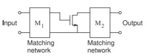
Figure \(\PageIndex{4}\): An amplifier with an active device and input \((\text{M}_{1})\) and output \((\text{M}_{2})\) matching networks. The biasing arrangement is not shown, but usually this is done with the appropriate choice of matching network topology.
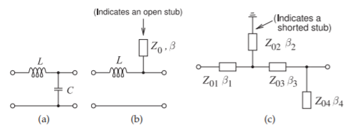
Figure \(\PageIndex{5}\): Three forms of matching networks with increasing use of transmission line sections.
For the usual case where all of the reference transmission lines have the same characteristic impedance \(Z_{0} = 1/Y_{0}\) (note \(S =\:^{N}\mathbf{S}\)),
\[\label{eq:60}\mathbf{Y}=Y_{0}(\mathbf{U}-\mathbf{S})(\mathbf{U}+\mathbf{S})^{-1}\quad\text{and}\quad\mathbf{S}=(\mathbf{Y}_{0}+\mathbf{Y})^{-1}(\mathbf{Y}_{0}-\mathbf{Y}) \]