
6.5: Dealing with Complex Loads
- Page ID
- 41137
This section presents strategies for dealing with complex loads. In the algorithmic matching approach design proceeds first by ignoring the complex load and source and then accounting for them either through topology choice or canceling their effect through resonance.
6.5.1 Matching
Input and output impedances of transistors, mixers, antennas, etc., contain both resistive and reactive components. Thus a realistic impedance matching problem looks like that shown in Figure 6.4.9. The matching approaches that were presented in the previous sections can be directly applied if \(X_{S}\) and \(X_{L}\) are treated as stray reactances that need to be either canceled or, ideally, used as part of the matching network. There are two basic approaches to handling complex impedances:
- Absorption: Absorb source and load reactances into the impedance matching network itself. This is done through careful placement of each matching element such that capacitors are placed in parallel with source and load capacitances, and inductors in series with source and load inductances. The stray values are then subtracted from the \(L\) and \(C\) values for the matching network calculated on the basis of the resistive parts of \(Z_{S}\) and \(Z_{L}\) only. The new (smaller) values, \(L'\) and \(C'\), constitute the elements of the matching network. Sometimes it is necessary to perform a series-to-parallel, or parallel-to-series, conversion of the source or load impedances so that the reactive elements are in the correct series or shunt arrangement for absorption.
- Resonance: Resonate source and load reactances with an equal and opposite reactance at the frequency of interest.
The very presence of a reactance in a load indicates energy storage, and therefore bandwidth limiting of some kind. In the above approaches to handling a reactive load, the resonance approach could easily result in a narrowband matching solution. The major problem in matching is often to obtain sufficient bandwidth. What is sufficient will vary depending on the application. To maximize bandwidth the general goal is to minimize the total energy storage. Roughly the total energy stored will be proportional to the sum of the magnitudes of the reactances in the circuit. Of course, the actual energy storage depends on the voltage and current levels, which will themselves vary in the circuit. A good approach leading to large bandwidths is to incorporate the load reactance into the matching network. Thus the choice of appropriate matching network topology is critical. However, if the source and load reactance value is larger than the calculated matching network element value, then absorption on its own cannot be used. In this situation resonance must be combined with absorption. Overall, the majority of impedance matching designs are based on some combination of resonance and absorption.
Example \(\PageIndex{1}\): Matching Network Design Using Resonance
For the configuration shown in Figure \(\PageIndex{1}\), design an impedance matching network that will block the flow of DC current from the source to the load. The frequency of operation is \(1\text{ GHz}\). Design the matching network, neglecting the presence of the \(10\text{ pF}\) capacitance at the load. Since \(R_{S} = 50\:\Omega < R_{L} = 500\:\Omega\), and from Figure 6.4.2, consider the topologies of Figures \(\PageIndex{2}\)(a) and \(\PageIndex{2}\)(b). The design criterion of blocking flow of DC from the source to the load narrows the choice to the topology of Figure \(\PageIndex{2}\)(b).
Solution
Step 1:
\[\label{eq:1}|Q_{S}|=\left|\frac{X_{S}}{R_{S}}\right|=|Q_{P}|=\left|\frac{R_{L}}{X_{P}}\right|=\sqrt{\frac{R_{L}}{R_{S}}-1}=3\quad\text{and}\quad Q_{P}=\frac{R_{L}}{X_{P}} \]
So \(X_{P} = \omega L = R_{L}/Q_{P} = 500/3\). Reducing this gives
\[\label{eq:2}\omega L=\frac{500}{3},\quad\text{and so}\quad L=\frac{500}{3\times 2\pi\times 10^{9}}=26.5\text{ nH} \]
Similarly \(−X_{S}/R_{S} = 3\) and so
\[\label{eq:3}\frac{1/(\omega C)}{R_{S}}=3\quad\text{or}\quad C=\frac{1}{3\omega R_{S}}=\frac{1}{3\times 2\pi\times 10^{9}\times 50}=1.06\text{ pF} \]
Step 2:
Resonate the \(10\text{ pF}\) capacitor using an inductor in parallel:
\[\begin{align}\label{eq:4}(\omega L')^{-1}&=\omega\times 10\times 10^{-12} \\ \label{eq:5}L'&=\frac{1}{\omega ^{2}10^{-11}}=\frac{1}{(2\pi )^{2}10^{18}\times 10^{-11}}=2.533\text{ nH}\end{align} \]
Thus Figure \(\PageIndex{2}\)(c) is the required matching network. Two inductors are in parallel and the circuit can be simplified to that shown in Figure \(\PageIndex{3}\), where
\[\label{eq:6} L_{X}=(26.5\text{ nH}\parallel 2.533\text{ nH})=\frac{2.533\times 26.5}{2.533+26.5}\text{ nH}=2.312\text{ nH} \]
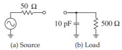
Figure \(\PageIndex{1}\): Matching problem considered in Example \(\PageIndex{1}\).
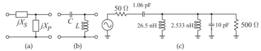
Figure \(\PageIndex{2}\): Matching network topology used in Example \(\PageIndex{1}\): a) and (b) topology; and (c) intermediate matching network.
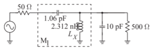
Figure \(\PageIndex{3}\): Final matching network in Example \(\PageIndex{1}\).
Example \(\PageIndex{2}\): Matching Network Design Using Resonance and Absorption
For the source and load configurations shown in Figure \(\PageIndex{4}\), design a lowpass impedance matching network at \(f = 1\text{ GHz}\).
Solution
Since \(R_{S} < R_{L}\), use the topology shown in Figure \(\PageIndex{5}\)(a). For a lowpass response, the topology is that of Figure \(\PageIndex{5}\)(b). Notice that absorption is the natural way of handling the \(3\text{ nH}\) at the source and the \(5\text{ pF}\) at the load. The design process is as follows:
Step 1:
Design the matching network, neglecting the reactive elements at the source and load:
\[\label{eq:7}|Q_{S}|=|Q_{P}|=\sqrt{\frac{R_{L}}{R_{S}}-1}=\sqrt{10-1}=3 \]
\[\begin{align}\label{eq:8}\frac{X_{S}}{R_{S}}&=3,\quad X_{S}=3\times 100,\quad \omega L=300\quad\text{and}\quad L=\frac{300}{2\pi\times 10^{9}}=47.75\text{ nH} \\ \label{eq:9}\frac{R_{P}}{X_{P}}&=-3\quad\text{and}\quad\frac{1000}{-(1/\omega C)}=-3\quad\text{and}\quad C=\frac{3}{1000\times 2\pi\times 10^{9}}=0.477\text{ pF}\end{align} \]
This design is shown in Figure \(\PageIndex{6}\)(a). This is the matching network that matches the \(100\:\Omega\) source resistance to the \(1000\:\Omega\) load with the source and load reactances ignored.
Step 2:
Figure \(\PageIndex{6}\)(b) is the interim matching solution. The source inductance is absorbed into the matching network, reducing the required series inductance of the matching network. The capacitance of the load cannot be fully absorbed. The design for the resistance-only case requires a shunt capacitance of \(0.477\text{ pF}\), but \(5\text{ pF}\) is available from the load. Thus there is an excess capacitance of \(4.523\text{ pF}\) that must be resonated out by the inductance \(L''\):
\[\label{eq:10}\frac{1}{\omega L''}=\omega 4.523\times 10^{-12}.\quad\text{So}\quad L''=\frac{1}{(2\pi)^{2}\times 10^{18}\times 4.523\times 10^{-12}}=5.600\text{ nH} \]
The final matching network design (Figure \(\PageIndex{6}\)(c)) fully absorbs the source inductance into the matching network, but only partly absorbs the load capacitance.
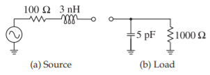
Figure \(\PageIndex{4}\): Matching problem in Example \(\PageIndex{2}\).
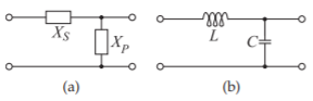
Figure \(\PageIndex{5}\): Topologies referred to in Example \(\PageIndex{2}\).
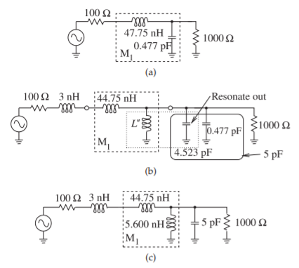
Figure \(\PageIndex{6}\): Evolution of the matching network in Example \(\PageIndex{2}\): (a) matching network design considering only the source and load resistors; (b) matching network with the reactive parts of the source and load impedances included; and (c) final design.