
6.9: Matching Options Using the Smith Chart
- Page ID
- 41141
The purpose of this section is to use the Smith chart to present several design options for matching a source to a load, see Figure \(\PageIndex{1}\). The designs here provide another view of design using the Smith chart.
6.9.1 Locating the Design Points
The first design choice to be made is the reference impedance to use. Here \(Z_{\text{REF}} = 50\:\Omega\) will be chosen largely because this is in the center of the design space for microstrip lines. Generally the characteristic impedance, \(Z_{0}\), of a microstrip line needs to be between \(20\:\Omega\) and \(100\:\Omega\). A microstrip line with \(Z_{0} < 20\:\Omega\) will be wide and there is a possibility of multimoding due to transverse resonance. Also \(20\:\Omega\) line is about six times wider than a \(50\:\Omega\) line and so takes up a lot of room and there is a good chance that it could be close to other microstrip lines or perhaps the wall of an enclosure. This is based on the rule of thumb (developed in Example 3.4.1 of [1]) that \(Z_{0} ∝ \sqrt{h/w}\) where \(h\) is the substrate thickness and \(w\) is the strip width. The thickness is usually fixed, i.e. it is not always a readily changed design choice. If \(Z_{0} > 100\:\Omega\) the characteristic impedance is getting close to the wave impedance of free space and of the dielectric of the substrate. As such it is likely that field lines are not tightly constrained by the metal of the strip and the fields can more likely radiate. Then radiation loss can be high or coupling to a neighboring microstrip can be high.
The normalized source and load impedances are \(z_{S} = Z_{S}/Z_{\text{REF}} = [(29.36 − \jmath 12.05)\:\Omega ]/(50\:\Omega) = 0.587 − \jmath 0.241\) and \(z_{L} = Z_{L}/Z_{\text{REF}} = [(132.7 − \jmath 148.8)\:\Omega /(50\:\Omega ) = 2.655 −\jmath 2.976 = r_{L} + \jmath x_{L},\) respectively. Maximum power transfer requires that the input impedance of the matching network terminated in \(Z_{L}\) be \(Z_{1} = Z_{S}^{\ast},\) i.e. \(z_{1} = z_{S}^{\ast} = 0.587 +\jmath 0.241 = r_{1} + \jmath x_{1}\). These impedances are plotted on the normalized Smith chart in Figure \(\PageIndex{2}\). The normalized load impedance is Point \(\mathsf{L}\). To locate this point the arcs corresponding to the real and imaginary parts of \(z_{L}\) are considered separately. The resistive part of \(z_{L}\) is \(r_{L} = 2.655\) and the resistance labels are
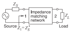
Figure \(\PageIndex{1}\): Matching problem with the matching network between the source and load designed for maximum power transfer. \(Z_{S} = R_{S} + \jmath X_{S} = 29.36 − \jmath 12.05,\) \(Z_{1} = R_{1} + \jmath X_{1} = Z_{S}^{\ast} = R_{S} − \jmath X_{S} = 29.36 + \jmath 12.05,\) and \(Z_{L} = R_{L} + \jmath X_{L} = 32.7 − \jmath 148.8\).
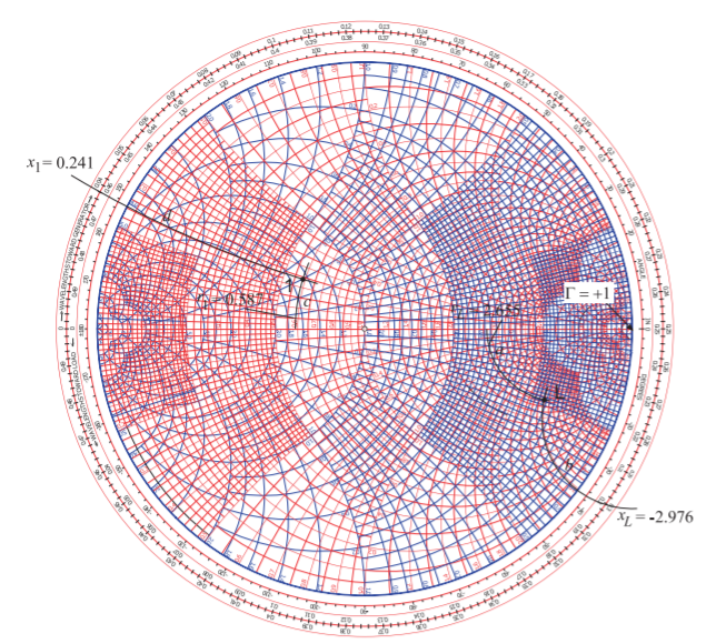
Figure \(\PageIndex{2}\): Locating \(Z_{L}\) at Point \(\mathsf{L}\) and \(Z_{1} = Z_{S}^{\ast}\) at Point \(\mathsf{1}\).
located on the horizontal axis (or equator) of the Smith chart. There are two sets of labels, one for normalized resistance, \(r\) (which is above the horizontal axis), and one for normalized conductance, \(g\) (which is below the horizontal axis). The way to remember which is which is to realize that the infinite impedance point is at the \(\Gamma = +1\) (open circuit) location on the right of the graph. At the origin (center) of the Smith chart \(r =1= g\) and to the right of the center the values of \(r\) should be greater than one. The closest \(r\) labels to \(r_{L} = 2.655\) are \(r = 2.0\) and \(r = 3.0\). There are five divisions so the unlabeled curves correspond to \(2.2, 2.4,\ldots\). The arc corresponding to \(r = 2.655\) must be interpolated and this interpolation is shown as the Path ‘\(\mathsf{a}\)’.
The imaginary part of \(z_{L}\) is \(x_{L} = −2.976\). The labels for the arcs of constant reactance are given adjacent to the unit circle. There are two sets of labels, one for reactance and one for susceptance. To recall which is which, the point of infinite impedance can be used and the required reactance labels should increase towards the \(\Gamma = +1\) point. Recall that the Smith chart does not include signs of reactances (there is not enough room) so note must be made that positive reactances are in the top half of the Smith chart and negative reactances are in the bottom half. Since \(x_{L}\) is negative it will be in the bottom half of the Smith chart. The closest labels are \(x = 2.0\) (this is actually \(−2.0\)) and \(x = 3.0\) (this is actually \(−3.0\)) so the arc for \(x = −2.976\) is interpolated as the Path ‘\(\mathsf{b}\)’. Point \(\mathsf{L}\), i.e. \(z_{L}\), is located at the intersection of Paths ‘\(\mathsf{a}\)’ and ‘\(\mathsf{b}\)’. The normalized impedance \(z_{1}\) is located similarly at Point \(\mathsf{1}\) by finding the point of intersection of the \(r_{1} = 0.587\) arc, Path ‘\(\mathsf{c}\)’, and the \(x_{1} = +0.241\) arc, Path ‘\(\mathsf{d}\)’.
6.9.2 Design Options
By convention design follows a process of beginning with \(z_{L}\) and adding series and shunt elements in front of it evolving the impedance (or reflection coefficient) until the input impedance is \(z_{1} = z_{S}^{\ast}\). Three electrical designs are shown in Figure \(\PageIndex{3}\) and the corresponding lumped-element and microstrip topologies are shown in Figure \(\PageIndex{4}\). The subscript on the circuit elements correspond to the paths on the Smith chart in Figure \(\PageIndex{3}\). The designs will be elaborated in the following subsections.
6.9.3 Design 1, Hybrid Design
Design 1 on its own is shown in Figure \(\PageIndex{5}\). The concept here is to use a transmission line and a shunt to go from the load Point \(\mathsf{L}\) to the Point \(\mathsf{1}\). The reason why a shunt element is chosen and not a series element is that the shunt element can be implemented as stub line and a series element, i.e. a series stub, cannot be implemented in microstrip. A lumped element limits a design to the low microwave range as losses become prohibitively large especially for inductors. Also if a microstrip line is going to be used anyway then a decision already has been made that there is enough room to implement a transmission-line based design and so the shunt lumped element can reasonably be replaced by a stub.
Design follows trial and error. The first attempt, and the one that works here, is to draw a circle through \(\mathsf{L}\) centered on the origin at Point \(\mathsf{O}\). This circle describes a transmission line whose characteristic impedance is the same as the reference impedance of the Smith chart, here \(50\:\Omega\). The next step is to draw a circle of constant conductance through Point \(\mathsf{1}\). The combination path from \(\mathsf{L}\) to \(\mathsf{1}\) needs to lie on these circles and the intermediate point will be where these circles intersect. One other constraint is that with a transmission line the locus (as the line length increases) of the input reflection coefficient of the line must rotate in the clockwise direction. It is seen that there are two points of intersection and the first of these, at \(\mathsf{A}\), is chosen in design. So the electrical design is defined by the directed Paths ‘\(\mathsf{g}\)’ and ‘\(\mathsf{h}\)’. Path ‘\(\mathsf{g}\)’ defines the properties of the transmission line and Path ’\(\mathsf{h}\)’ defines the properties of the shunt element. As ‘\(\mathsf{h}\)’ is directed towards the infinite inductive susceptance point, Path ‘\(\mathsf{h}\)’ defines an inductor. The topology of this design is shown in Figure \(\PageIndex{4}\)(a).
The characteristic impedance of the transmission line (defined by Path ‘\(\mathsf{g}\)’) is \(Z_{0g} = 50\:\Omega\). The electrical length of the line is defined by the angle subtended by the arc ‘\(\mathsf{g}\)’. The electrical length of the line is determined from the outermost circular scale which is labeled ‘WAVELENGTHS TOWARDS
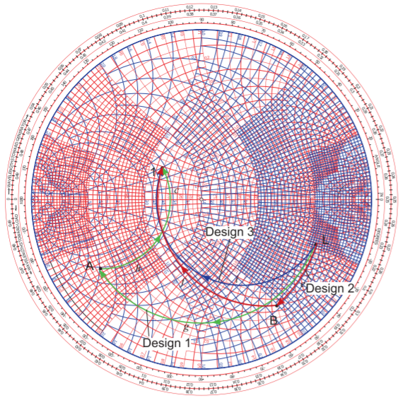
Figure \(\PageIndex{3}\): Three matching network electrical designs matching a load impedance \(Z_{L}\) at Point \(\mathsf{L}\) to a source \(Z_{S}\) showing \(Z_{1} = Z_{S}^{\ast}\) at Point \(\mathsf{1}\).
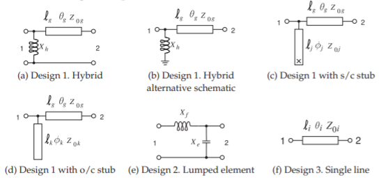
Figure \(\PageIndex{4}\): Matching network topologies using lumped elements and microstrip lines. In the stub layouts \(\mathsf{x}\) is a via to the ground plane implementing a short circuit (s/c) and an open circuit o/c simply does not show a connection to the microstrip ground plane.
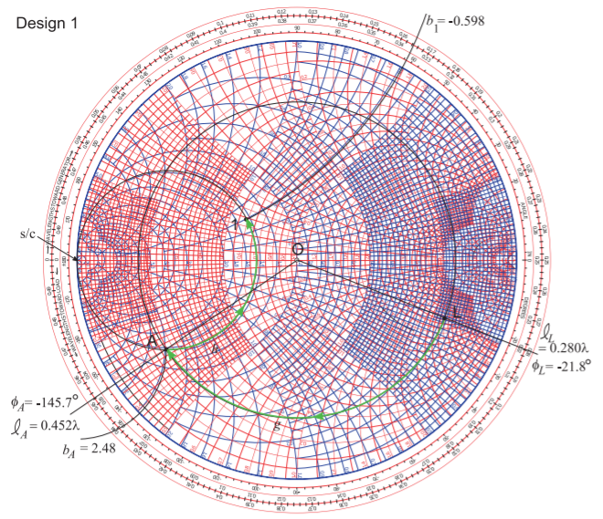
Figure \(\PageIndex{5}\): Design 1. Hybrid design combining a transmission line with a lumped element in shunt. The design is identified by paths ‘\(\mathsf{g}\)’ and ‘\(\mathsf{h}\)’.
GENERATOR.’ A line drawn from \(\mathsf{O}\) through \(\mathsf{L}\) intersecting the scale has a scale reading of \(\ell_{L} = 0.280\lambda\). Then the scale reading at \(\mathsf{A}\) is similarly found as \(\ell_{A} = 0.452\lambda\) and so the line length is \(\ell_{g} = \ell_{A} −\ell_{L} = 0.452\lambda −0.280\lambda = 0.172\lambda\). Another way of determining the electrical length of the line is from the change in reflection coefficient angle. For \(\mathsf{L}\) the reflection coefficient angle is \(\phi_{L} = −21.8^{\circ}\) read from the innermost circular scale. This angle is just the angle from the polar plot. Then the angle at \(\mathsf{A}\) is read as \(\phi_{A} = −145.7^{\circ}\). The difference is \(|\phi_{A} −\phi_{L}| = |−145.7−(−21.8^{\circ})| = 124.9^{\circ}\). The electrical length of the line is half the change in reflection coefficient angle and so the electrical length of the line is \(\theta_{g} = \frac{1}{2} 124.9^{\circ} = 62.5^{\circ}\). Now \(\lambda\) corresponds to an electrical length of \(360^{\circ}\) so \(\theta_{g}\) corresponds to \(62.5/360\lambda = 0.174\lambda\) corresponding to the previously determined length of \(0.172\lambda\) which is very good agreement given that these were derived from graphical readings.
Path ‘\(\mathsf{h}\)’ defines a shunt inductor and a circle of constant conductance is followed with only the susceptance changing. The susceptance indicated by Path ‘\(\mathsf{g}\)’ is \(b_{g} = b_{1} −b_{A}\). To obtain \(b_{A}\) extend the circle of constant susceptance through \(\mathsf{A}\) out to the unit circle. The extended circle cross the unit circle between the susceptance labels \(2.0\) and \(3.0\). A check is that susceptance is positive in the bottom half of the Smith chart so the signs of the labels do not need to be adjusted. There are two scales adjacent to the unit circle, one for normalized susceptance and one for normalized reactance. Since the intersection is close to the infinite susceptance point at the s/c (shortcircuit) so the values that are becoming very large towards s/c are used. Interpolation results in the reading \(b_{A} = 2.48\). A similar process applied to Point \(\mathsf{1}\) results in \(b_{1} = −0.598\) where the negative sign has been applied to the scale reading since the point of intersection between the arc of constant susceptance passing through Point \(\mathsf{1}\) and the unit circle is in the top half of the Smith chart. Thus \(b_{h} = b_{1} − b_{A} = −0.598 − 2.48 = −3.08\) and so the normalized reactance of the shunt element is \(x_{h} = −1/b_{h} = 0.325\). The unnormalized reactance of the shunt element is \(X_{h} = x_{h}Z_{\text{REF}} = 16.2\:\Omega\).
The final Design 1 hybrid layout is shown in Figure \(\PageIndex{4}\)(a) with \(X_{h} = 16.2\:\Omega\), \(Z_{0g} = 50\:\Omega\), and \(\ell_{g} = 0.172\lambda\). That is all that is needed to define the electrical design, providing the electrical length in degrees, \(\theta_{g} = 62.5^{\circ}\) is redundant but provided anyway. The transmission line in Figure \(\PageIndex{4}\)(a) is shown as as the top view of the strip of a microstrip line as is commonly done. A more common way of representing this schematic is shown in Figure \(\PageIndex{4}\)(b) where the ground connections at Ports \(\mathsf{1}\) and \(\mathsf{2}\) have been removed and the ground connection of the inductor shown separately.
6.9.4 Design 1 with an Open-Circuited Stub
In the previous section Design 1 was left as a hybrid design with a transmission line and a lumped-element inductor. In this section the lumped-element inductor is implemented as an open-circuited stub, see Figure \(\PageIndex{4}\)(d). Recall that the \(50\:\Omega\)-normalized susceptance of the inductor is \(b_{h} = −3.08\). If the stub is also implemented as a \(50\:\Omega\) line then \(b_{h}\) can be used unchanged. Point \(\mathsf{C}\) in Figure \(\PageIndex{6}\) corresponds to the normalized admittance \(0 −\jmath 3.08\). The unit circle is the zero conductance circle (and is also the zero resistance circle) and the susceptance is read from the scale adjacent to the unit circle again using as reference that susceptances in the top half of the Smith chart need to incorporate a negative sign and the susceptance scale is identified by the susceptance values becoming larger approaching the s/c point. Point \(\mathsf{C}\) also corresponds to \(x_{h} = −1/b_{h} = 3.25\) and indeed this is the value read from the normalized reactance scale.
A transmission line needs to be designed to have a normalized input susceptance of \(b_{h} = −3.08\). Choosing an open circuit, o/c, termination the point corresponding to o/c is as identified in the figure. At the o/c point the length scale reads \(\ell_{\text{o/c}} = 0.250\lambda\). The locus rotates in the clockwise direction up to Point \(\mathsf{C}\) where the direct electrical reading reading is \(\ell_{C} = 0.050\lambda\). Using this directly to determine the line length \(\ell_{k} = \ell_{C} − \ell_{\text{o/c}} = 0.050\lambda − 0.250\lambda = −0.20\lambda\) which indicates that the stub has a negative length. Clearly an erroneous result. This apparent discrepancy comes about because the length scale resets at the short circuit point where the length scale abruptly goes from \(0.5\lambda\) to \(0\lambda\). Thus the corrected \(\ell_{C}\) reading needs to have an additional \(0.5\lambda\). Thus the corrected value of \(\ell_{C} = (0.5+0.050)\lambda = 0.550\lambda\)
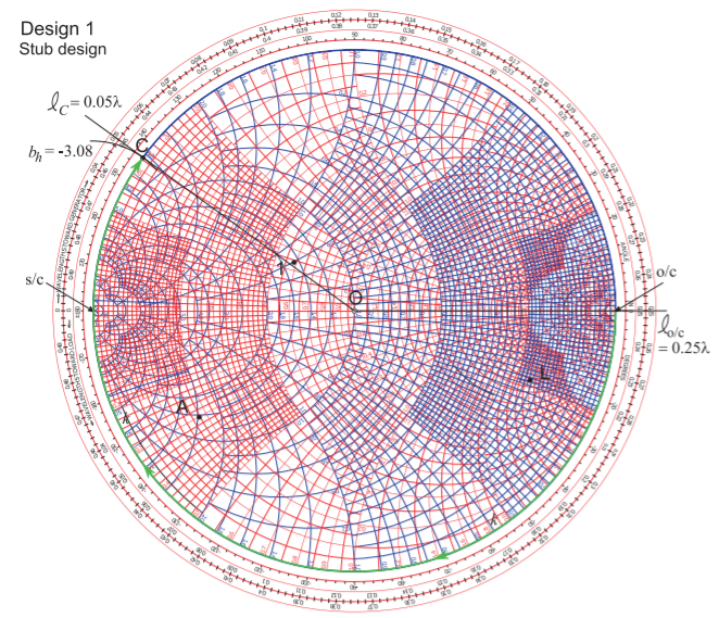
Figure \(\PageIndex{6}\): Design 1. Design of an open-circuit stub having normalized input susceptance \(b_{h}\).
and \(\ell_{k} = \ell_{C} − \ell_{\text{o/c}} = 0.550\lambda − 0.250\lambda = 0.300\lambda\).
Thus the final design is as shown in Figure \(\PageIndex{4}\)(d) with \(Z_{0k} = 50\:\Omega\), and \(\ell_{g} = 0.300\lambda,\: Z_{0g} = 50\:\Omega\), and \(\ell_{g} = 0.172\lambda\).
The stub could also have been implemented as a short-circuit stub as shown in Figure \(\PageIndex{4}\)(c). Now the beginning of the line would be at the s/c point and the line length would be \(0.050\lambda\).
6.9.5 Design 2, Lumped-Element Design
Design 2 is a lumped-element design and the Smith-chart-based electrical design is shown in Figure \(\PageIndex{7}\) resulting in the schematic shown in Figure \(\PageIndex{4}\)(e). Design proceeds by identifying where circles of constant conductance and constant resistance passing through the Points \(\mathsf{L}\) and \(\mathsf{1}\) intersect. One solution is shown in Figure \(\PageIndex{7}\). A circle of constant conductance passes through \(\mathsf{L}\) and part of a circle of constant resistance passes through \(\mathsf{1}\). If the circle had continued there would have been a second intersection with
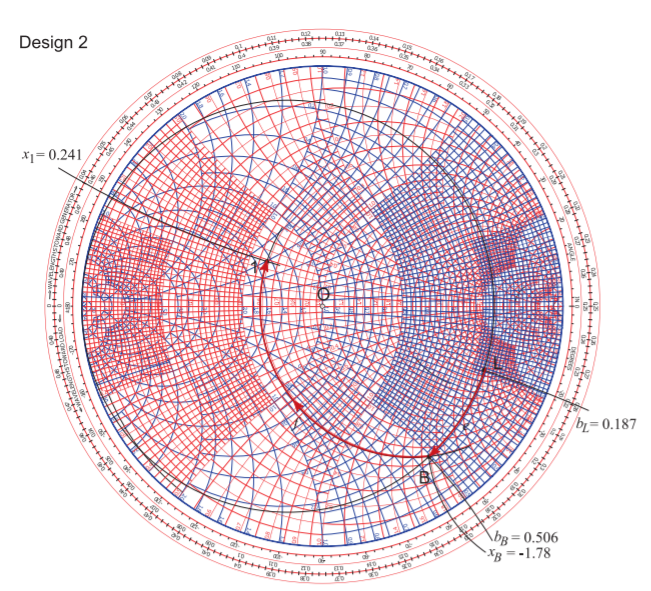
Figure \(\PageIndex{7}\): Design 2.
the circle through \(\mathsf{L}\). Both of these intersections mean that there is a shunt element adjacent to the load and series element adjacent to the source. Recall that in a lumped-element design that under no circumstances can the locus of a lumped element pass through the short circuit point (if it is a susceptance) or open-circuit point (if it is a reactance), the susceptance and reactance infinity points respectively.
Returning to the actual design shown in Figure \(\PageIndex{7}\). The first intersection of the two circles is Point \(\mathsf{B}\) so that the design is specified by the Paths ‘\(\mathsf{e}\)’ and ’\(\mathsf{f}\)’. Design has largely been completed by identifying these paths and the next stage is determining the circuit elements that correspond to these paths. Path ‘\(\mathsf{e}\)’ follows a circle of constant conductance and so indicates a shunt susceptance and the direction of the locus indicates a capacitance. The value of this normalized susceptance is \(b_{e} = b_{B} −b_{L} = 0.506−0.187 = 0.319\). (Remember to check the signs of the readings since the Smith chart omits signs of the reactances and susceptances.) Path ‘\(\mathsf{f}\)’ identifies a series inductor with a reactance \(x_{f} = x_{1} − x_{B} = 0.241 − (−1.78) = 2.02\). The final design is shown in Figure \(\PageIndex{4}\)(e) with \(X_{e} = Z_{0}/b_{e} = 50/0.319\:\Omega = 158\:\Omega\) and \(X_{f} = Z_{0}x_{f} = 50\cdot 2.02\:\Omega = 101\:\Omega\).
6.9.6 Design 3, Single Line Matching
Design 3 uses a single transmission line to match the source and load as shown in the schematic of Figure \(\PageIndex{4}\)(f). This design is akin to using a quarter-wave transmission line transformer but with a Smith chart being used the approach can now be used with complex source and load impedances. Recall from Sections 3.5.2 and 4.5 that the locus of a terminated transmission line is a circle on the Smith chart even if the characteristic impedance of the transmission line, \(Z_{0i}\) in Design 3, and the reference impedance, \(Z_{\text{REF}}\), are not the same. Furthermore the center of the circle will be on the horizontal axis. The Smith-chart-based electrical design of Design 3 is shown in Figure \(\PageIndex{8}\) where \(Z_{\text{REF}} = 50\:\Omega\). There is only one way to draw a circle that passes through two points with the center of the circle constrained to be on the horizontal axis. That circle is shown in Figure \(\PageIndex{8}\) with Path ‘\(\mathsf{i}\)’ on the circle going from Points \(\mathsf{L}\) to \(\mathsf{1}\) tracing out the locus of the reflection coefficient. This locus must be in the clockwise direction. The center of the circle is at Point \(\mathsf{D}\) and the center of the circle is (the reflection coefficient normalized to \(Z_{\text{REF}}\)) is \(C_{D} = 0.240\). (The radius is also given but this is not necessary.) The angle subtended by Path ‘\(\mathsf{i}\)’ is twice the electrical length of the line. This angle cannot be directly measured from the scales (although it is possible by placing a chart over the top and and aligning the center of the polar plot with \(\mathsf{D}\)) and here was read using a protractor. The angle is \(\phi_{D} = 150^{\circ}\) so that the electrical length of the line is \(\theta_{i} = \frac{1}{2} 150^{\circ} = 75^{\circ}\), i.e. \(\ell_{i} = 74/360\lambda = 0.208\lambda\). The only parameter not known is the characteristic impedance, \(Z_{0i}\), of the line. This must be arrived at iteratively. From Equation (4.5.3) (after replacing \(Z_{01},\: Z_{02}\) and \(C_{Z02}\) by \(Z_{0i},\: Z_{\text{REF}}\) and \(C_{D}\), respectively)
\[\label{eq:1}Z_{0i}\approx Z_{\text{REF}}(1+C_{D})/(1-C_{D}) \]
with the approximation improving the closer \(Z_{0i}\) is to \(Z_{\text{REF}}\). Substituting \(Z_{\text{REF}} = 50\:\Omega\) and \(C_{D} = 0.240\), the first iteration of \(Z_{0i}\) is
\[\label{eq:2} ^{1}Z_{0i}=50\left(\frac{1+0.240)}{1-0.240)}\right)\:\Omega=82\:\Omega \]
Re-plotting using a new reference impedance of \(Z_{\text{REF}} = 82\:\Omega\) yields a new center of \(0.07\) from which an updated iterate is \(^{2}Z_{0i} = 94\:\Omega\) and then a new center of \(0.02\) and \(^{3}Z_{0i} = 98\:\Omega\). Continuing to iterate results in an asymptotic value \(Z_{0i} = 100\:\Omega\). \(Z_{0i}\) can also be estimated from the tabulated values in Table 4.5.1. Reading the line with radius of \(0.5\) and center of \(0.24\) yields \(Z_{0i} = 50\cdot 1.980 = 99\:\Omega\).
The final design is as shown in Figure \(\PageIndex{4}\)(f) with \(\ell_{i} = 0.208\lambda,\:\theta_{i} = 75^{\circ}\), and \(Z_{0i} = 100\:\Omega\).
As was seen with the quarter-wave transformer design using multiple stages significantly increases bandwidth by matching to intermediate resistances determined as geometric means of the source and load resistance. The corresponding strategy here is to draw a line between the Points \(\mathsf{1}\) and \(\mathsf{L}\) and, if there are to be two stages, choose the intermediate matching impedance
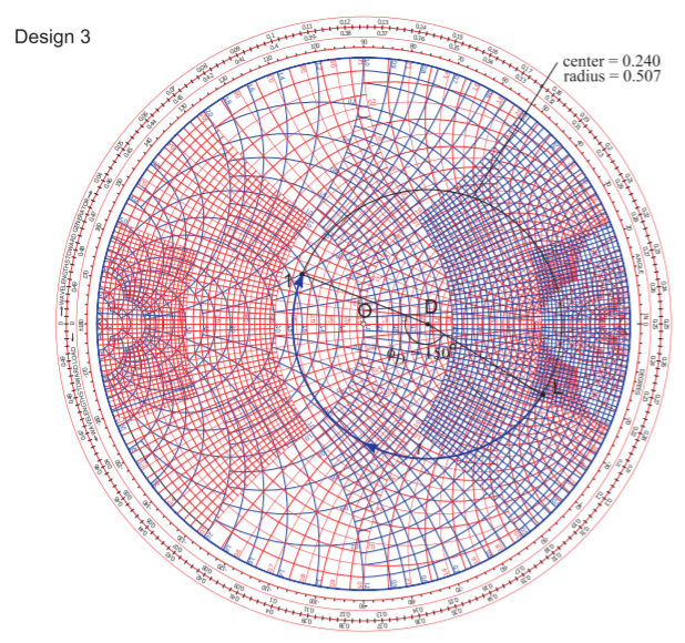
Figure \(\PageIndex{8}\): Design 3.
at the mid-point of the line. If the source and loads are complex then the reactive storage elements in the source and load will set a limit on maximum achievable bandwidth.
6.9.7 Summary
This section presented three quite different designs for a matching network. One of the particular benefits of using the Smith chart is identifying topologies and initial design values. Design can then transfer to a microwave circuit simulator. The Smith chart enables back-of-the-envelope design studies. While with experience it is possible to complete many of these steps with a computer-based Smith chart tool, even experienced designers doodle with a printed Smith chart when exploring design options.