
7.4: Stepped-Impedance Transmission Line Transformer
- Page ID
- 41146
The wideband matching techniques described in this section use multiple quarter-wavelength-long transmission line sections with the lines having characteristic impedances which are stepped from the source impedance to the load impedance. They are conceptual extensions of the quarter-wave transformer and differ by how the characteristic impedances of the sections are chosen. The methods strictly are applicable to resistive source and load impedances yet achieve reasonably wideband matches with moderately reactive source and load impedances.
7.4.1 Quarter-Wave Transformer using Geometric Means
Design here uses multiple quarter-wave long transmission lines the characteristic impedances of which are chosen as geometric means of the source and load impedances. The procedure is described in the next example.
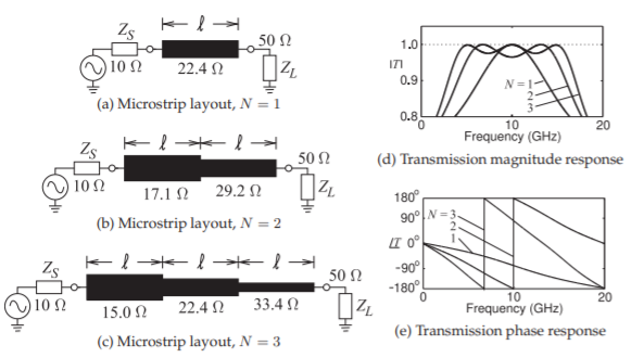
Figure \(\PageIndex{1}\): Transmission line transformer designed in Example \(\PageIndex{1}\). Each section is of length \(\ell = \lambda_{g}/4=2.83\text{ mm}\) where \(\lambda_{g}\) is the midband wavelength (at \(10\text{ GHz}\)).
Example \(\PageIndex{1}\): Multisection Quarter-Wave Transmission Line Transformer
Design one-, two, and three-section quarter-wave transformers in microstrip to connect a power amplifier with an output impedance of \(10\:\Omega\) to a \(50\:\Omega\) cable.
Solution
The parameters are \(Z_{S} = 10\:\Omega\) and \(Z_{L} = 50\:\Omega\). The characteristic impedance of a single, \(N = 1\), quarter-wave transformer is \(Z_{01} =\sqrt{Z_{S}Z_{L}} = 22.36\:\Omega\).
With a two-section, \(N = 2\), quarter-wave transformer (using geometric means)
\[Z_{01}=\sqrt[3]{Z_{S}^{2}Z_{L}}=17.10\:\Omega\quad Z_{02}=\sqrt[3]{Z_{S}Z_{L}^{2}}=29.24\:\Omega\nonumber \]
With a three-section, \(N = 3\), quarter-wave stepped-impedance transformer
\[\label{eq:1}Z_{01}=\sqrt{Z_{S}Z_{02}}=14.95\:\Omega\quad Z_{02}=\sqrt{Z_{S}Z_{L}}=22.36\:\Omega\quad Z_{03}=\sqrt{Z_{02}Z_{L}}=33.44\:\Omega \]
The microstrip layouts are shown in Figure \(\eqref{eq:1}\) where each section is a quarter-wavelength long at mid band. The simulated transmission characteristics of the design realized at \(10\text{ GHz}\) (on alumina, \(\varepsilon_{r} = 10,\) and attenuation of \(1.87\text{ dB/m}\) are shown in Figure \(\PageIndex{1}\)(d and e).
7.4.2 Design Based on the Theory of Small Reflections
Another design method for choosing the characteristic impedances of cascaded lines is based on the theory of small reflections [4, 5]. The reflection coefficients at each boundary in Figure \(\PageIndex{2}\) are defined as
\[\label{eq:2}\Gamma_{0}=\frac{Z_{01}-Z_{S}}{Z_{01}+Z_{S}}\quad\Gamma_{n}=\frac{Z_{n+1}-Z_{n}}{Z_{n+1}+Z_{n}}\quad\Gamma_{N}=\frac{Z_{L}-Z_{0N}}{Z_{L}+Z_{0N}} \]
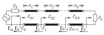
Figure \(\PageIndex{2}\): Stepped-impedance transmission line transformer with the \(n\)th section having characteristic impedance \(Z_{0n}\) and electrical length \(\theta_{n}\). \(\Gamma_{n}\) is the reflection coefficient, and \(Z_{n}\) the impedance, considering only the \((n + 1)\)th line.
As these are small reflections (since \(Z_{0n}\) changes gradually) the theory of small reflections (described in Section 2.6.5 of [6]) can be invoked and so, using Equation ((2.201) of [6]), the total reflection coefficient seen from the source \(Z_{S}\) is
\[\label{eq:3}\Gamma_{\text{in}}\approx\Gamma_{0}+\text{e}^{-2\jmath\theta_{1}}(\Gamma_{1}+\text{e}^{-2\jmath\theta_{2}}(\Gamma_{2}+\cdots\text{e}^{-2\jmath\theta_{N}}\Gamma_{N})) \]
It is now necessary to make a design choice. It has been found that a multisection transformer that provides a good broadband match at both the source and load has symmetrical reflection coefficients, i.e. \(\Gamma_{n} = \Gamma_{N−n}\) [5]. Another design choice is that the electrical lengths of the sections are the same, i.e. \(\theta_{n} =\theta\). Then Equation \(\eqref{eq:3}\) becomes
\[\begin{align}\label{eq:4}\Gamma_{\text{in}}&=\Gamma_{0}+\Gamma_{1}\text{e}^{-2\jmath\theta_{1}}+\Gamma_{2}\text{e}^{-4\jmath\theta_{2}}+\cdots\Gamma_{N}\text{e}^{-2\jmath N\theta_{N}}\\ &=\Gamma_{0}\left[1+\text{e}^{-2\jmath N\theta}\right]+\Gamma_{1}\left[\text{e}^{-2\jmath\theta}+\text{e}^{-2\jmath (N-1)\theta}\right]+\ldots \\ &=\text{e}^{-\jmath N\theta}\left\{\Gamma_{0}\left[\text{e}^{\jmath N\theta}+\text{e}^{-\jmath N\theta}\right]+\Gamma_{1}\left[\text{e}^{\jmath (N-2)\theta}+\text{e}^{-\jmath (N-2)\theta}\right]+\ldots\right\}\nonumber \\ \label{eq:5}&=2\text{e}^{-\jmath N\theta}\left\{\Gamma_{0}\cos(N\theta)+\Gamma_{1}\cos[(N-2)\theta]+\ldots\right\}\end{align} \]
using the trigonometric identity \(\cos x =\frac{1}{2}(\text{e}^{\jmath x} + \text{e}^{−\jmath x})\) (and this is where symmetry is used). The last term in Equation \(\eqref{eq:5}\) is \(\frac{1}{2}\Gamma_{N/2}\) if \(N\) is even and \(\Gamma_{(N−1)/2} \cos\theta\) if \(N\) is odd.The design variables here are the reflection coefficients at each line boundary (from which the characteristic impedances of the lines can be found) and the mid-band electrical length \(\theta_{0}\).
The general design approach is to assume a functional form for \(\Gamma_{\text{in}}(\theta)\) and then to derive the \(\Gamma_{n}\)s that result in that functional form. \(\Gamma_{\text{in}}(\theta)\) will now be used to indicate that \(\Gamma_{\text{in}}\) is a function of \(\theta\) and hence of frequency. Also the mid-band electrical length \(\theta_{0}\) is set to \(\pi /2\) corresponding to the sections being a quarter-wavelength long. This may seem arbitrary but it has been shown to be optimum [7] (for maximum bandwidth). The final design step is to derive the characteristic impedances of the line sections. Using Equation \(\eqref{eq:2}\)
\[\label{eq:6}Z_{0N}=Z_{L}\left(\frac{1-\Gamma_{N}}{1+\Gamma_{N}}\right)\quad\text{and}\quad Z_{0n}=Z_{0(n+1)}\left(\frac{1-\Gamma_{n}}{1+\Gamma_{n}}\right) \]
7.4.3 Maximally Flat Stepped Impedance Transformer
The design objective here is to set the first \(N\) derivatives of \(\Gamma_{\text{in}}\) at midband to zero. This results in a very smooth response and that is what is desired in some situations. If the following assignment is made
\[\label{eq:7}|\Gamma_{\text{in}}(\theta)|\propto |\cos(\theta)|^{N} \]
then \(d^{n}|\Gamma_{\text{in}}(\theta)|/d\theta^{n} = 0\) at \(\theta = \pi /2 = \theta_{0}\) for \(n = 0, 1,\ldots ,(N − 1)\). An assignment that results in this is the binomial expansion
\[\label{eq:8}\Gamma_{\text{in}}(\theta)=A(1+\text{e}^{-2\jmath\theta})^{N}=\sum_{n=0}^{N}\left(\begin{array}{c}{N}\\{n}\end{array}\right)\text{e}^{-2\jmath n\theta} \]
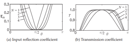
Figure \(\PageIndex{3}\): Characteristics of order \(N = 1,\: 2,\: 3\) and \(4\) maximally flat stepped-impedance transformers with an impedance mismatch \(\delta_{z} = \text{max}(Z_{L}/Z_{S},\: Z_{S}/Z_{L})=2\).
where (since \(N\) and \(n\) are integers)
\[\label{eq:9}\left(\begin{array}{c}{N}\\{n}\end{array}\right)=\frac{N!}{(N-n)!n!} \]
is the binomial coefficient. Equating Equations \(\eqref{eq:4}\) and \(\eqref{eq:8}\)
\[\label{eq:10}\Gamma_{n}=A\left(\begin{array}{c}{N}\\{n}\end{array}\right) \]
To find \(A\) consider zero frequency. Then \(\theta = 0\) and the transformer has no effect and \(\Gamma_{\text{in}}\) is just the mismatch of the source and load impedances and Equation \(\eqref{eq:8}\) becomes
\[\label{eq:11}\Gamma_{\text{in}}(0)=A2^{N}=\frac{Z_{L}-Z_{S}}{Z_{L}+Z_{S}}\quad\text{so that}\quad A=2^{-N}\left(\frac{Z_{L}-Z_{S}}{Z_{L}+Z_{S}}\right) \]
Thus
\[\label{eq:12}\Gamma_{n}(\theta)=2^{-N}\left(\frac{Z_{L}-Z_{S}}{Z_{L}+Z_{S}}\right)\left(\begin{array}{c}{N}\\{n}\end{array}\right) \]
and \(Z_{0n}\) comes from Equation \(\eqref{eq:6}\) with the design accuracy determined by the approximation of a small discontinuity at each transmission line boundary.
The reflection \(\Gamma_{\text{in}}\) and transmission \(T\) characteristics of maximally flat stepped-impedance transformers are shown in Figure \(\PageIndex{3}\) for various orders. As with all lossless two-ports \(|T| =\sqrt{1 − |\Gamma_{\text{in}}|^{2}}\). It can be seen that the bandwidth increases with increasing order and the transmission is remarkably flat.
Example \(\PageIndex{2}\): Maximally Flat Multisection Transmission Line Transformer
Design a three-section maximally flat stepped-impedance transformer in microstrip to connect a \(Z_{S} =5\:\Omega\) source to a \(Z_{L} = 50\:\Omega\) load.
Solution
The design will have three transmission lines of different characteristic impedance and each section will be a quarter-wavelength long at mid band. Now \(N = 3\) so from Equation \(\eqref{eq:12}\)
\[\begin{align} \label{eq:13}\Gamma_{n}&=2^{-N}\left(\frac{Z_{L}-Z_{S}}{Z_{L}+Z_{S}}\right)\left(\begin{array}{c}{N}\\{n}\end{array}\right) =2^{-3}\left(\frac{50-5}{50+5}\right)\left(\begin{array}{c}{3}\\{n}\end{array}\right)=\frac{45}{8\cdot 55}\left(\begin{array}{c}{3}\\{n}\end{array}\right) \\ \Gamma_{3}&=0.1023\frac{3!}{0!3!}=\frac{1}{16}\frac{3\cdot 2\cdot 1}{1\cdot 3\cdot 2\cdot 1}=0.1023,\quad \Gamma_{2}=0.3068,\quad\Gamma_{1}=0.3068,\quad\Gamma_{0}=0.1023\end{align} \nonumber \]
resulting in (a sanity check is the expectation that \(Z_{L} > Z_{03} > Z_{02}\ldots\))
\[Z_{03}=50\frac{1-0.1023}{1+0.1023}\:\Omega=40.72\:\Omega,\quad Z_{02}=21.60\:\Omega,\quad Z_{01}=11.46\:\Omega,\quad\text{and}\quad Z_{S}'=9.333\:\Omega\nonumber \]
where \(Z_{S}'\) is ideally (the complex conjugate of) the original \(Z_{S}\) but is actually significantly different. This is because the design is based on the theory of small reflections and so multiple reflections at the transmission line boundaries were not considered. As a further investigation, and noting that each section is a quarter-wavelength long at midband, another estimate for \(Z_{S}\), call this \(Z_{S}''\), is found using Equation ((2.132)) of [6],
\[Z_{2}=Z_{03}^{2}/Z_{L}=33.16\:\Omega,\quad Z_{1}=Z_{02}^{2}/Z_{2}=14.07\:\Omega,\quad Z_{S}''=Z_{01}^{2}/Z_{1}=9.334\:\Omega\nonumber \]
The microstrip layout is shown in Figure \(\PageIndex{4}\)(a). Simulation of the design realized at \(10\text{ GHz}\) (on alumina, \(\varepsilon_{r} = 10,\) a \(2.83\text{ mm}\) section length, and a line attenuation of \(1.87\text{ dB/m}\) for an overall attenuation of \(0.016\text{ dB}\)) results in the transmission characteristics identified by \(\delta_{z} = Z_{L}/Z_{S} = 10\) in Figure \(\PageIndex{4}\)(b). The final design does not have the ideal maximally flat transmission characteristics and this is due to deficiencies in the small reflection assumption. Final design requires a small amount of optimization as the synthesized design has a maximum in-band insertion loss of \(0.4\text{ dB}\) \((T = 0.953)\).
Repeating the design with \(Z_{S} = 10\:\Omega\) and \(Z_{L} = 50\:\Omega\) results in \(\Gamma_{0} =\Gamma_{3} = 0.08333,\) \(\Gamma_{1} =\Gamma_{2} = 0.2500,\) \(Z_{01} = 15.23\:\Omega ,\) \(Z_{02} = 25.38\:\Omega\), \(Z_{03} = 42.31\:\Omega\), and \(Z_{S}' = Z_{S}'' = 12.89\:\Omega\). The transmission characteristics are identified by \(\delta_{z} = Z_{L}/Z_{S} = 5\) in Figure \(\PageIndex{4}\)(b). The minimum in-band transmission coefficient is \(0.990\) for a maximum insertion loss of \(0.091\text{ dB}\). Thus design accuracy improves for a lower impedance transformation ratio.
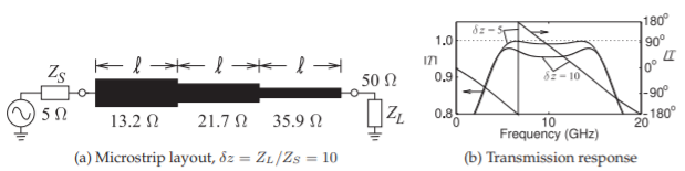
Figure \(\PageIndex{4}\): Maximally flat transmission line transformer designed in Example \(\PageIndex{2}\). At \(10\text{ GHz}\) each section is of length \(\ell = \lambda_{g}/4=2.83\text{ mm}\) where \(\lambda_{g}\) is the midband wavelength.
7.4.4 Stepped Impedance Transformer with Chebyshev Response
Expressing the input reflection coefficient \(\Gamma_{\text{in}}\) of a stepped-impedance transformer in terms of a Chebyshev polynomial results in a good match in-band that rapidly transitions outside the passband. Compared to the maximally flat transformer a much better match can be obtained for the same number of line sections if the resulting ripples in the passband can be tolerated. With reference to Equation \(\eqref{eq:3}\), the design choice is
\[\begin{align} \Gamma_{\text{in}}(\theta)&=\Gamma_{0}+\text{e}^{-2\jmath\theta}(\Gamma_{1}+\text{e}^{-2\jmath\theta}(\Gamma_{2}+\cdots\text{e}^{-2\jmath\theta}\Gamma_{N}))\nonumber \\ \label{eq:14}&=A\text{e}^{-\jmath N\theta}T_{N}(\cos\theta /\cos\theta_{m})\end{align} \]
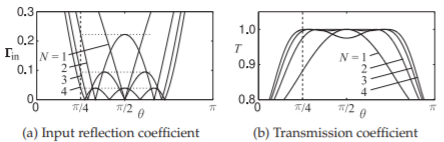
Figure \(\PageIndex{5}\): Characteristics of order \(N = 1,\: 2,\: 3\) and \(4\) Chebyshev stepped-impedance transformers with impedance mismatch \(\delta_{z} = \text{max}(Z_{L}/Z_{S},\: Z_{S}/Z_{L}) = 2\) and \(\theta_{m} = \pi/4\). The transmission ripple cannot be seen for \(N\geq 3\).
where \(T_{N}\) is the \(N\)th order Chebyshev polynomial of the first kind (as described in Section 1.A.10 of [6]). In Equation \(\eqref{eq:14}\) \(\theta_{m}\) defines the passband of the transformer as being between \(\theta_{m}\leq\theta\leq (\pi −\theta_{m})\) and in the passband \(|\Gamma_{\text{in}}(\theta )|\leq\Gamma_{m}\) and at \(\theta =\theta_{m}\) and \(\theta = (\pi − \theta_{m})\) (the edges of the passband)
\[\begin{align}\label{eq:15} |\Gamma_{\text{in}}(\theta_{m})|=|\Gamma_{\text{in}}(\pi -\theta_{m})|&=\Gamma_{m}=|AT_{N}(\cos\theta_{m}/\cos\theta_{m})|=|AT_{N}(1)| \\ \label{eq:16}\text{Since }|T_{N}(1)|=1\quad A&=\Gamma_{m}\end{align} \]
To proceed another expression is needed for A so that \(\Gamma_{m},\: N,\) and \(\theta_{m}\) (and thus bandwidth) can be related. This is obtained by considering the mismatch at zero frequency, that is when \(\theta = 0\):
\[\label{eq:17}\Gamma_{\text{in}}(0)=\left|\frac{Z_{L}-Z_{S}}{Z_{L}+Z_{S}}\right|=AT_{N}(\sec\theta_{m}) \]
(where \(\sec\theta_{m} = 1/ \cos\theta_{m}\)) and so
\[\label{eq:18}A=\left|\frac{Z_{L}-Z_{S}}{Z_{L}+Z_{S}}\right|\frac{1}{T_{N}(\sec\theta_{m})} \]
Substituting for A in Equation \(\eqref{eq:14}\) and using Equation \(\eqref{eq:3}\) results in
\[\begin{align}\text{e}^{\jmath N\theta}\Gamma_{\text{in}}(\theta)&=AT_{N}(\cos\theta /\cos\theta_{m})=\left(\frac{Z_{L}-Z_{S}}{Z_{L}+Z_{S}}\right)\frac{T_{N}(\cos\theta/\cos\theta_{m})}{T_{N}(\sec\theta_{m})}\nonumber \\ \label{eq:19}&=2\left\{\Gamma_{0}\cos (N\theta)+\Gamma_{1}\cos[(N-2)\theta]+\ldots\right\}\end{align} \]
The expansion of \(T_{N} (\cos\theta/ \cos\theta_{m})\) is given in Equation ((1.198)) of [6] and has terms in \(\cos(m\theta)\) and so design (which requires \(\Gamma_{n}\)) proceeds by equating terms in Equation \(\eqref{eq:19}\) having the same \(\cos(m\theta )\) for \(m = 1,\ldots ,N\). This will be illustrated in an example.
The reflection \(\Gamma_{\text{in}}\) and transmission \(T\) characteristics of Chebyshev stepped-impedance transformers are shown in Figure \(\PageIndex{5}\) for orders from one to four for \(\theta_{m} = \pi/4\) (this indicates a \(100\%\) bandwidth). It is seen that the maximum inband \(\Gamma_{\text{in}}\)) reduces with increasing order. So with a Chebyshev response there is a trade-off between passband ripple and bandwidth.
An expression for bandwidth of the match will now be developed. Equating Equations \(\eqref{eq:16}\) and \(\eqref{eq:18}\)
\[\label{eq:20}T_{N}(\sec\theta_{m})=\frac{1}{\Gamma_{m}}\left|\frac{Z_{L}-Z_{S}}{Z_{L}+Z_{S}}\right| \]
Using the identity
\[\label{eq:21}T_{N}(\sec\theta_{m})=\cosh (N\cosh^{-1}(\sec\theta_{m}))=\frac{1}{\Gamma_{m}}\left|\frac{Z_{L}-Z_{S}}{Z_{L}+Z_{S}}\right| \]
| \(N=\) | \(1\) | \(1\) | \(1\) | \(2\) | \(2\) | \(2\) | \(3\) | \(3\) | \(3\) | \(4\) | \(4\) | \(4\) | \(5\) | \(5\) | \(5\) |
|---|---|---|---|---|---|---|---|---|---|---|---|---|---|---|---|
| \(\Gamma_{m}\) | \(0.05\) | \(0.1\) | \(0.151\) | \(0.05\) | \(0.1\) | \(0.151\) | \(0.05\) | \(0.1\) | \(0.151\) | \(0.05\) | \(0.1\) | \(0.151\) | \(0.05\) | \(0.1\) | \(0.151\) |
| \(\delta_{Z}\) | Fractional bandwidth, \(\Delta f/f_{0}\) | ||||||||||||||
| \(1.0\) | \(∞\) | \(∞\) | \(∞\) | \(∞\) | \(∞\) | \(∞\) | \(∞\) | \(∞\) | \(∞\) | \(∞\) | \(∞\) | \(∞\) | \(∞\) | \(∞\) | \(∞\) |
| \(1.2\) | \(0.741\) | \(∞\) | \(∞\) | \(1.275\) | \(∞\) | \(∞\) | \(1.502\) | \(∞\) | \(∞\) | \(1.622\) | \(∞\) | \(∞\) | \(1.696\) | \(∞\) | \(∞\) |
| \(1.3\) | \(0.501\) | \(1.112\) | \(∞\) | \(1.069\) | \(1.526\) | \(∞\) | \(1.346\) | \(1.680\) | \(∞\) | \(1.500\) | \(1.759\) | \(∞\) | \(1.596\) | \(1.807\) | \(∞\) |
| \(1.4\) | \(0.388\) | \(0.819\) | \(1.441\) | \(0.951\) | \(1.333\) | \(1.714\) | \(1.252\) | \(1.544\) | \(1.808\) | \(1.425\) | \(1.655\) | \(1.856\) | \(1.534\) | \(1.722\) | \(1.885\) |
| \(1.6\) | \(0.278\) | \(0.571\) | \(0.907\) | \(0.814\) | \(1.134\) | \(1.395\) | \(1.137\) | \(1.396\) | \(1.588\) | \(1.330\) | \(1.540\) | \(1.689\) | \(1.455\) | \(1.629\) | \(1.750\) |
| \(1.8\) | \(0.224\) | \(0.455\) | \(0.708\) | \(0.735\) | \(1.024\) | \(1.250\) | \(1.066\) | \(1.310\) | \(1.483\) | \(1.271\) | \(1.471\) | \(1.607\) | \(1.405\) | \(1.573\) | \(1.684\) |
| \(2.0\) | \(0.192\) | \(0.388\) | \(0.598\) | \(0.683\) | \(0.951\) | \(1.158\) | \(1.018\) | \(1.252\) | \(1.415\) | \(1.229\) | \(1.424\) | \(1.554\) | \(1.369\) | \(1.534\) | \(1.641\) |
| \(2.5\) | \(0.149\) | \(0.300\) | \(0.458\) | \(0.604\) | \(0.844\) | \(1.026\) | \(0.943\) | \(1.162\) | \(1.313\) | \(1.164\) | \(1.351\) | \(1.607\) | \(1.313\) | \(1.472\) | \(1.574\) |
| \(3.0\) | \(0.128\) | \(0.256\) | \(0.390\) | \(0.561\) | \(0.784\) | \(0.954\) | \(0.900\) | \(1.110\) | \(1.254\) | \(1.125\) | \(1.307\) | \(1.426\) | \(1.280\) | \(1.436\) | \(1.535\) |
| \(4.0\) | \(0.106\) | \(0.213\) | \(0.324\) | \(0.513\) | \(0.718\) | \(0.874\) | \(0.850\) | \(1.051\) | \(1.188\) | \(1.081\) | \(1.257\) | \(1.372\) | \(1.241\) | \(1.393\) | \(1.490\) |
| \(6.0\) | \(0.085\) | \(0.179\) | \(0.271\) | \(0.471\) | \(0.660\) | \(0.804\) | \(0.805\) | \(0.997\) | \(1.128\) | \(1.040\) | \(1.211\) | \(1.322\) | \(1.204\) | \(1.354\) | \(1.449\) |
| \(8.0\) | \(0.082\) | \(0.164\) | \(0.249\) | \(0.452\) | \(0.634\) | \(0.772\) | \(0.784\) | \(0.971\) | \(1.100\) | \(1.020\) | \(1.189\) | \(1.299\) | \(1.187\) | \(1.335\) | \(1.429\) |
| \(10\) | \(0.078\) | \(0.156\) | \(0.236\) | \(0.441\) | \(0.618\) | \(0.754\) | \(0.772\) | \(0.957\) | \(1.083\) | \(1.009\) | \(1.176\) | \(1.285\) | \(1.176\) | \(1.323\) | \(1.417\) |
Table \(\PageIndex{1}\): Relationship of order \(N\), fractional bandwidth, impedance ratio \(\delta_{z} = \text{max}(Z_{L}/Z_{S},\: Z_{S}/Z_{L}),\) and reflection coefficient ripple \(\Gamma_{m}\) for a Chebyshev stepped-impedance transformer. A transmission ripple of \(0.1\text{ dB}\) has \(\Gamma_{m} = 0.151\). (For example, a two-section \((N = 2)\) transformer has a \(95.4\%\) bandwidth with \(\delta_{z} = 3.0\).)
and so
\[\label{eq:22}\theta_{m}=\sec^{-1}\left\{\cosh\left[\frac{1}{N}\cosh^{-1}\left(\frac{1}{\Gamma_{m}}\left|\frac{Z_{L}-Z_{S}}{Z_{L}+Z_{S}}\right|\right)\right]\right\} \]
The fractional bandwidth can be obtained by noting that \(\theta\) and thus \(\theta_{m}\) are proportional to frequency \(f\). That is, \(f = k\theta\). At the passband center frequency \(f_{0},\:\theta = \pi /2\) and so \(k = 2f_{0}/\pi\). Thus if \(f_{m}\) is the frequency at the lower band edge, \(f_{m} = k\theta_{m} = 2f_{0}\theta_{m}/\pi\). Then the fractional bandwidth (with the passband defined by when \(|\Gamma_{\text{in}}|\leq\Gamma_{m}\)) is
\[\label{eq:23}\frac{\Delta f}{f_{0}}=\frac{2(f_{0}-f_{m})}{f_{0}}=2-\frac{4\theta_{m}}{\pi} \]
Thus Equations \(\eqref{eq:22}\) and \(\eqref{eq:23}\) relate the fractional bandwidth, the maximum passband reflection coefficient \(\Gamma_{m}\), the impedance mismatch \(\delta_{z} = \text{max}(Z_{L}/Z_{S},\: Z_{S}/Z_{L})\), and the Chebyshev order, \(N\). Table \(\PageIndex{1}\) enables the required transformer order to be selected for a specified bandwidth and impedance mismatch.
Example \(\PageIndex{3}\): Chebyshev Multisection Transmission Line Transformer
Design a \(100\%\) bandwidth three-section Chebyshev stepped-impedance transformer in microstrip to connect a power amplifier with an output impedance of \(10\:\Omega\) to a \(50\:\Omega\) cable.
Solution
The design parameters are \(N = 3,\: Z_{S} = 10\:\Omega,\) and \(Z_{L} = 50\:\Omega\). From Equation \(\eqref{eq:23}\) the fractional bandwidth \(\Delta f /f_{0} =1=2 − (4\theta_{m})/\pi\) so that \(\theta_{m} = \pi /4\). Then, with \(\sec\theta_{m} = 1/ \cos\theta_{m} = 1/ \cos(\pi /4) =\sqrt{2}\) and \(T_{3}(\sqrt{2}) = 7.071\) (from Equation ((1.193) of [6])), Equation \(\eqref{eq:18}\) yields
\[\label{eq:24}\Gamma_{m}=A=\left(\frac{Z_{L}-Z_{S}}{Z_{L}+Z_{S}}\right)\frac{1}{T_{3}(\sec\theta_{m})}=\left(\frac{50-10}{50+10}\right)\frac{1}{7.071}=0.09418 \]
Using Equation \(\eqref{eq:19}\) and the Chebyshev expansion for \(T_{3}\) this leads to
\[\begin{align} AT_{3}(\cos\theta /\cos\theta_{m})&=A\left\{\sec^{3}\theta_{m}[\cos (3\theta)+3\cos\theta]-3\sec\theta_{m}\cos\theta\right\} \nonumber \\ \label{eq:25}&=2[\Gamma_{0}\cos(3\theta)+\Gamma_{1}\cos(\theta)]\end{align} \]
Thus after equating like terms in \(\cos(m\theta)\) (noting that \(\Gamma_{n} = \Gamma_{(N−n)}\) since symmetry is required)
\[\begin{align}\Gamma_{0}&=\Gamma_{3}=\frac{1}{2}A\sec^{3}\theta_{m}=\frac{1}{2}0.09428\cdot\left(\sqrt{2}\right)^{3}=0.1333\nonumber \\ \label{eq:26}\Gamma_{1}&=\Gamma_{2}=\frac{3}{2}A\left[\sec^{3}\theta_{m}-\sec\theta_{m}\right]=\frac{3}{2}0.09428\cdot\left[\left(\sqrt{2}\right)^{3}=\sqrt{2}\right]=0.2000\end{align} \]
Then the characteristic impedances of the three line sections are (using Equation \(\eqref{eq:6}\))
\[\label{eq:27}Z_{01}=13.19\:\Omega ,\quad Z_{02}=21.78\:\Omega ,\quad\text{and}\quad Z_{03}=35.94\:\Omega \]
and each section is a quarter-wavelength long at midband. The microstrip layout is shown in Figure \(\PageIndex{6}\)(a). The simulated transmission characteristics of the design realized at \(10\text{ GHz}\) (on alumina, \(\varepsilon_{r} = 10,\) section lengths of \(2.83\text{ mm}\), and an attenuation of \(1.87\text{ dB/m}\) (for an overall attenuation of \(0.016\text{ dB}\)) are shown in Figure \(\PageIndex{6}\)(b). The expected lossless ripple (from \(T = \sqrt{1 −\Gamma_{m}^{2}} = 0.9955 = −0.039\text{ dB})\) is \(0.039\text{ dB}\). The simulated minimum insertion loss is \(0.024\text{ dB}\) and the maximum in-band insertion loss is \(0.057\text{ dB}\) for a passband ripple of \(0.033\text{ dB}\) (line loss is known to reduce ripple).
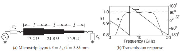
Figure \(\PageIndex{6}\): Chebyshev transformer of Example \(\PageIndex{3}\). (\(\lambda_{g}\) is the midband wavelength.)
7.4.5 Stepped Impedance Transformer Design
The multisection stepped-impedance transformers change the characteristic impedances of the section between the source and load resistances but do so in steps. It is possible to achieve a similar result by continuously tapering the characteristic impedance of the transmission line taper or, equivalently, tapering the width of microstrip line as shown in Figure \(\PageIndex{7}\).
7.4.6 Summary
The multisection impedance transformer design described in this section is based on transmission line sections each a quarter-wavelength long at the center frequency of the match. It is tempting to think that a better result could be obtained by having sections of various lengths. However it has been shown that optimum matching transformer designs are of the quarter-wave Chebyshev type and only minimum enhancement is possible [7].
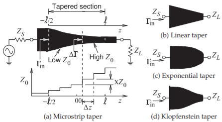
Figure \(\PageIndex{7}\): Tapered impedance transformers with length \(\ell\). The width of the microstrip line is approximately inversely proportional to the characteristic impedance of the line. (Here \(Z_{L} > Z_{S}\) and both \(Z_{L}\) and \(Z_{S}\) are resistive.)