
7.5: Tapered Matching Transformers
- Page ID
- 41147
Tapered impedance transformers match an impedance \(Z_{S}\) to an impedance \(Z_{L}\) using a transmission line having a characteristic impedance \(Z_{0}\) that gradually and monotonically varies from \(Z_{S}\) to \(Z_{L}\) along the length of the line, see Figure 7.4.7. This figure references a microstrip line but the key aspect is the gradual change in characteristic impedance that applies to any transmission line. The central design problem is how to choose the function \(Z_{0}(z)\). If the length of the line, \(\ell\) here, is not constrained then the Klopfentein taper [8, 9] is regarded as the optimum approach for design of the taper and will be discussed after first reviewing approaches used when the length of the line is constrained. Note that both \(Z_{L}\) and \(Z_{S}\) are resistive.
7.5.1 Small Reflection Theory and Tapered Lines
In this section the theory behind the synthesis of a taper is developed beginning with the theory of small reflections. The reflection at point \(z\) on the line for a taper segment of length \(\Delta z\) is (refer to Figure 7.4.7(a))
\[\label{eq:1}\Delta\Gamma=\frac{(Z_{0}(z)+\Delta z)-Z_{0}(z)}{(Z_{0}+\Delta Z)+Z_{0}(z)}=\frac{\Delta Z}{2Z_{0}(z)+\Delta Z}\approx\frac{\Delta Z}{2Z_{0}(z)} \]
where \(Z_{0}(z)\) is the characteristic impedance of the taper at \(z\) and \(\Delta Z\) is the change of \(Z_{0}(z)\) from one side of the taper segment to the other. In the limit as \(\Delta Z\to 0,\) \(\Delta Z\) is replaced by \(dZ\) and \(\Delta\Gamma\) is replaced by \(d\Gamma\) so that Equation \(\eqref{eq:1}\) becomes (and putting in differential operator form)
\[\label{eq:2}d\Gamma=\frac{dZ_{0}}{2Z_{0}(z)}\quad\to\quad\frac{d\Gamma}{dz}=\frac{\text{d}\Gamma}{\text{d}z}=\frac{1}{2Z_{0}(z)}\frac{\text{d}Z_{0}}{\text{d}z} \]
The next step is to refer all of the small reflections, \(\Delta\Gamma\), to the beginning of the taper at \(z = −\ell /2\). The theory of small reflections is that these small reflections, accounting for the electrical lengths from the start of the taper to each taper segment, can be summed, see Equation (7.4.3). This is the same as saying that the small reflection from one taper segment is not affected by its own reflection from another taper segment. Noting that the electrical length from the beginning of the taper to a taper segment at \(z\) is \(\theta = \beta(\ell /2 + z)\), the reflection at the input of the tapered line is found as
\[\begin{align}\label{eq:3}\Gamma_{\text{in}}(\ell)&=\int_{z=-\ell /2}^{z=\ell /2}\text{e}^{-2\jmath (\ell/2+\beta z)}\text{d}\Gamma \\ \label{eq:4}&=\frac{1}{2}\text{e}^{-\jmath\beta\ell}\int_{-\ell/2}^{\ell/2}\frac{\text{e}^{-2\jmath\beta z}}{Z_{0}(z)}\frac{\text{d}Z_{0}(z)}{\text{d}z}\text{d}z\end{align} \]
where \(\Gamma_{\text{in}}\) is shown explicitly as a function of the length of the taper. So the design problem becomes choosing the characteristic impedance function, \(Z_{0}(z)\) to provide the desired input reflection coefficient \(\Gamma_{\text{in}}\). This is difficult to achieve with the form of Equation \(\eqref{eq:4}\). The problem can be simplified by noting that (and introducing \(Z_{1}\) as a normalizing impedance so that the argument of \(\ln\) is dimensionless)
\[\begin{align}\frac{\ln (Z_{0}(z)/Z_{1})}{\text{d}z}&=\frac{Z_{1}}{Z_{0}(z)}\frac{\text{d}(Z_{0}(z)/Z_{1})}{\text{d}z}=\frac{Z_{1}}{Z_{0}(z)}\frac{1}{Z_{1}}\frac{\text{d}(Z_{0}(z)/Z_{1})}{\text{d}z}\nonumber \\ \label{eq:5}&=\frac{1}{Z_{0}(z)}\frac{\text{d}(Z_{0}(z)/Z_{1})}{\text{d}z}\end{align} \]
and so, making it clear that \(d\Gamma\) varies along the taper,
\[\label{eq:6}d\Gamma (z)=\frac{1}{2}\frac{\text{d}(Z_{0}(z)/Z_{1})}{\text{d}z}dz \]
Thus after assuming the form of \(Z_{0}(z)\), the incremental reflection coefficient \(d\Gamma\) is obtained using Equation \(\eqref{eq:3}\). Alternatively (after integrating Equation \(\eqref{eq:6}\)) a form for \(\Gamma_{\text{in}}\) can be assumed and \(d\Gamma (z)\) determined and then \(Z_{0}(z)\). This will become clearer below when specific tapers are considered.
7.5.2 Linear taper
In the linear tapered line design \(Z_{0}(z)\) varies linearly from the source impedance \(Z_{S}\) to \(Z_{L}\):
\[\label{eq:7}Z_{0}(z)=Z_{S}+(Z_{L}-Z_{S})z/\ell \]
This is often approximated in microstrip by a linear taper of the width of the microstrip line as shown in Figure 7.4.7(b). A simple expression for the input reflection coefficient is not available and so must be found from simulation.
This is the simplest taper and the taper performs better the greater its electrical length (i.e. at higher frequencies or longer physical length). The performance of the linear taper is compared to other tapers later.
7.5.3 Exponential taper
The exponential taper has an exponential taper of the line’s characteristic impedance. Setting
\[\label{eq:8}Z_{0}(z)=Z_{x}\text{e}^{az}\quad\text{with}\quad a=\frac{1}{\ell}\ln (Z_{L}/Z_{S})\quad\text{and}\quad Z_{x}=Z_{S}\text{e}^{-a\ell /2} \]
results in the input reflection coefficient, derived using Equation \(\eqref{eq:4}\),
\[\label{eq:9}\Gamma_{\text{in}}(\ell)=\frac{1}{2}Z_{x}\text{e}^{-\jmath\beta\ell}\int_{-\ell/2}^{\ell/2}\text{e}^{-2\jmath\beta z}\frac{\text{d}\ln(\text{e}^{az})}{\text{d}z}\text{d}z=\frac{1}{2}\ln(Z_{L}/Z_{S})\frac{\sin(\beta\ell)}{\beta\ell} \]
So \(\Gamma_{\text{in}}\) has a sinc function characteristic with the variations of \(\Gamma_{\text{in}}\) reducing as the taper becomes longer. The main problem with this taper comes from the abrupt impedance discontinuity at the \(Z_{L}\) end of the taper. This taper will not be considered further as the Klopfenstein taper considered next has much better performance.
7.5.4 Klopfenstein taper
The Klopfenstein taper [8, 9] results in a specified reflection coefficient ripple (and thus transmission ripple) above a minimum passband frequency. It is believed to achieve the minimum taper length over a passband defined by the maximum allowable reflection coefficient mismatch, \(\Gamma_{m}\), (and so minimum transmission loss) in the passband. The linear taper and most other tapers used in matching [10, 11] assume the form of a taper’s characteristic impedance profile and the broadband reflection and transmission characteristics are whatever results. In contrast the Klopfenstein taper derives the required impedance profile for a source and load impedance mismatch ratio \((Z_{L}/Z_{S})\) and \(\Gamma_{m}\).
Klopfenstein [8] showed that the input reflection coefficient of the taper could be expressed as the limiting form of a high-order Chebyshev polynomial. Thus the Klopfenstein taper has the passband ripples that occur with Chebyshev-based multi-section impedance transformers and Chebyshev filters. The maximum magnitude of the reflection coefficient in the passband is determined by the line length. The appropriate characteristic impedance is computed from [8, 9]
\[\begin{align}\ln Z_{0}(z)&=\ln\left(\sqrt{Z_{S}Z_{L}}\right)+\ln\left(\sqrt{Z_{L}/Z_{S}}\right)\cdot (\cosh A)^{-1} \nonumber \\ \label{eq:10}&\quad\times [A^{2}\phi(2z/\ell,A)+U(z-\frac{1}{2}\ell)+U(z+\frac{1}{2}\ell)-1]\end{align} \]
where \(U(x)\) is the unit step function so that \(U(x)=0\) for \(x < 0\) and \(U(x)=1\) for \(x\geq 0\).
The maximum reflection coefficient amplitude \(\Gamma_{m} = \rho_{0}/ \cosh\:A\) where \(\rho_{0} = (Z_{L} − Z_{S}/(Z_{L} + Z_{S})\) is the reflection coefficient when the load and source are directly connected. Klopfenstein found that this introduced a small error attributed to the limitation of the small reflection assumption. He determined that a better estimate is \(\rho_{0} =\frac{1}{2}\ln (Z_{L}/Z_{S})\). Thus
\[\label{eq:11}A=\cosh^{-1}[\ln(Z_{L}/Z_{S})/\Gamma_{m}] \]
That is, \(\Gamma_{m}\), the maximum reflection coefficient in the passband, and the mismatch, \(Z_{L}/Z_{S}\), determines \(A\). Substituting Equation \(\eqref{eq:11}\) in Equation \(\eqref{eq:10}\) yields
\[\begin{align}\ln Z_{0}(z)&=\ln\left(\sqrt{Z_{S}Z_{L}}\right)+\ln\left(\sqrt{Z_{L}/Z_{S}}\right)\Gamma_{m}\frac{(Z_{L}+Z_{S})}{(Z_{L}-Z_{S})} \nonumber \\ \label{eq:12}&\quad\times\left[ A^{2}\phi (2x/\ell, A)+U(z-\frac{1}{2}\ell)+U(z+\frac{1}{2}\ell)-1\right]\end{align} \]
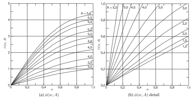
Figure \(\PageIndex{1}\): Klopfenstein taper function \(\phi (w, A)\) used in designing a taper segment. The taper has length \(\ell,\: z\) is the coordinate at the center of a taper segment, the center of the taper is at \(z = 0\), and \(\phi(−w,\: A) = −\phi (w,\: A),\: w = 2z/\ell\).
and the function \(\phi (w,\: A)\) is computed as [12]
\[\label{eq:13}\phi(w,\:A)=\sum_{k=0}^{\infty}a_{k}b_{k} \]
(summation up to \(k = 20\) is sufficient) with the recursion formulas
\[\label{eq:14}a_{0}=1,\: a_{k}=\frac{A^{2}}{4k(k+1)}a_{k-1};\quad b_{0}=\frac{1}{2}w,\quad b_{k}=\frac{\frac{1}{2}w(1-w^{2})^{k}+2kb_{k-1}}{2k+1} \]
The results are shown in Figure \(\PageIndex{1}\).
It is interesting to derive the characteristic impedance at the center of the taper. At the center of the taper, \(z = 0,\:\phi (0,\: A)=0\) and Equation \(\eqref{eq:10}\) becomes
\[\label{eq:15}\ln Z_{0}(0)=\frac{1}{2}\ln(Z_{S}Z_{L}),\quad\text{that is,}\quad Z_{0}(0)=\sqrt{Z_{S}Z_{L}} \]
which is the geometric mean of the source and load resistances.
The Klopfenstein taper trades off line length \(\ell\), minimum passband frequency \(f_{\text{min}}\), and maximum passband reflection coefficient \(\Gamma_{m}\). The passband of the taper is all frequencies above \(f_{\text{min}}\). This is a remarkable result with the line length being considerably less than that of a linear taper. The limitation is that with such a short line the reflections along the line cannot always be considered to be small so that it is often necessary to increase the line length slightly above the length derived from this synthesis procedure.
7.5.5 Simplified Klopfenstein taper
The simplified form of the Klopfenstein taper is obtained by noting that the acceptable value for the maximum in-band reflection coefficient \(\Gamma_{m}\) will
| \(w\) | Exact \(Z_{0}(w)/Z_{S}\) |
Simplified \(Z_{0}(w)/Z_{S}\) |
Error |
|---|---|---|---|
| \(-1.0\) | \(1.163\) | \(1.177\) | \(1.23\%\) |
| \(-0.8\) | \(1.326\) | \(1.344\) | \(1.32\%\) |
| \(-0.6\) | \(1.577\) | \(1.597\) | \(1.26\%\) |
| \(-0.4\) | \(1.944\) | \(1.964\) | \(1.04\%\) |
| \(-0.2\) | \(2.460\) | \(2.476\) | \(0.64\%\) |
| \(0.0\) | \(3.162\) | \(3.162\) | \(0\%\) |
| \(0.2\) | \(4.065\) | \(4.039\) | \(0.64\%\) |
| \(0.4\) | \(5.145\) | \(5.092\) | \(1.03\%\) |
| \(0.6\) | \(6.214\) | \(6.262\) | \(1.25\%\) |
| \(0.8\) | \(7.539\) | \(7.440\) | \(1.31\%\) |
| \(1.0\) | \(8.520\) | \(8.542\) | \(1.12\%\) |
Table \(\PageIndex{1}\): Comparison of \(Z_{0}\) of the exact and simplified Klopfenstein tapers (using Equation \(\eqref{eq:12}\) with Equations \(\eqref{eq:13}\) and \(\eqref{eq:16}\) respectively) for a maximum passband transmission loss \(T_{m} = 0.1\text{ dB}\) and \(Z_{L}/Z_{S} = 10\) \((\Gamma_{m} = 0.151\) and \(A = 2.72.)\) Errors are less for larger \(T_{m}\) and smaller \(Z_{L}/Z_{S}\):
For \(Z_{L}/Z_{S} = 20,\: T_{m} = 0.1\text{ dB}\), the max. error is \(2.78\%\).
For \(Z_{L}/Z_{S} = 20,\: T_{m} = 0.2\text{ dB}\), the max. error is \(1.49\%\).
For \(Z_{L}/Z_{S} = 10,\: T_{m} = 0.1\text{ dB}\), the max. error is \(1.33\%\).
For \(Z_{L}/Z_{S} = 10,\: T_{m} = 0.2\text{ dB}\), the max. error is \(0.66\%\).
For \(Z_{L}/Z_{S} = 5,\: T_{m} = 0.1\text{ dB}\), the max. error is \(0.44\%\).
For \(Z_{L}/Z_{S} = 5,\: T_{m} = 0.2\text{ dB}\), the max. error is \(0.21\%\).
typically be small and for a maximum transmission loss of between \(0.1\text{ dB}\) and \(1\text{ dB}\) (corresponding to \(\Gamma_{m} = 0.151\) and \(\Gamma_{m} = 0.454\) respectively) and maximum \(Z_{L}/Z_{S} = 10\). Then the maximum value of \(A\) is \(2.72\) and this is when the simplified Klopfenstein taper will have the most error. So retaining only the first three terms in Equation \(\eqref{eq:13}\), \(\phi(w,\: A)\) can be approximated as
\[\label{eq:16}\phi(w,\: A)=a_{0}b_{0}+a_{1}b_{1}+a_{2}b_{2} \]
and used in Equation \(\eqref{eq:12}\). A comparison of the calculated impedances for a relatively high transmission loss of \(1\text{ dB}\) (\(0.1\text{ dB}\) is more typical) and a large impedance mismatch \(Z_{L}/Z_{S} = 10\) is given in Table \(\PageIndex{1}\). The maximum error of \(1.33\%\) is comparable to the characteristic impedance error of fabricated transmission lines. So for practical purpose the simplified approach can be used to design the Klopfenstein taper.
Example \(\PageIndex{1}\): Design of a Klopfenstein Taper
Design a microstrip Klopfenstein taper to match a \(Z_{S} = 10\:\Omega\) source to a \(Z_{L} = 50\:\Omega\) load. The maximum transmission ripple is to be \(0.1\text{ dB}\) and the minimum passband frequency is \(8\text{ GHz}\). The substrate has a thickness \(h = 0.635\:\mu\text{m}\), and relative permittivity \(\varepsilon_{r} = 10.0\).
Solution
First determine the maximum reflection coefficient \(\Gamma_{m}\) in the passband. The minimum transmission in the passband is \(T = 10^{0.1/20}\) and \(\Gamma_{m} =\sqrt{1 − T^{2}} = 0.151\). Since \(Z_{L}/Z_{S} = 5\) it is seen from Table \(\PageIndex{1}\) that the simplified Klopfenstein taper can be used with a maximum error of \(1.33\%\). Using Equation \(\eqref{eq:11}\) the required electrical length of the taper at \(8\text{ GHz}\) is
\[A=\cosh^{-1}[\ln(Z_{L}/Z_{S})/\Gamma_{m}]=\cosh^{-1}[\ln(50/5)/0.151]=2.720\nonumber \]
A taper with ten segments is chosen and in the table below the normalized length \(w′ = 2z/\ell\) is used to distinguish the parameter from the microstrip width \(w\). The microstrip parameters were obtained by interpolating Table 3-3 of [6]. \(\overline{Z}_{0}\) and \(\overline{\varepsilon}_{e}\) are the average characteristic impedance and effective permittivity of a segment, a linear taper, extending from the width on the previous line to that on the same line. The electrical length of each segment is \(\beta (\Delta\ell ) = A/10 = 0.272\text{ radians}\) so that the physical length of a segment \(\ell = 0.272\lambda_{8\text{ GHz}}/(2π\sqrt{\varepsilon_{e}})\) where \(\lambda_{8\text{ GHz}} = 3.745\text{ cm}\) is the free-space wavelength at \(8\text{ GHz}\).
| Segment | \(w'\) | \(\phi (w',\: A)\) | \(Z_{0}\:(\Omega )\) | \(u=h/w\) | \(w\text{ (mm)}\) | \(\overline{Z}_{0}\:(\Omega)\) | \(\overline{\varepsilon}_{e}\) | \(\Delta\ell\text{ (}\mu\text{m)}\) |
|---|---|---|---|---|---|---|---|---|
| \(-1.0\) | \(−0.774\) | \(11.68\) | \(8.28\) | |||||
| \(1\) | \(-0.8\) | \(−0.661\) | \(12.84\) | \(7.38\) | \(12.2\) | \(8.35\) | ||
| \(2\) | \(-0.6\) | \(−0.521\) | \(14.44\) | \(6.39\) | \(14.1\) | \(8.19\) | ||
| \(3\) | \(-0.4\) | \(−0.360\) | \(16.52\) | \(5.40\) | \(16.0\) | \(8.05\) | ||
| \(4\) | \(-0.2\) | \(−0.184\) | \(19.16\) | \(4.45\) | \(17.8\) | \(7.93\) | ||
| \(5\) | \(0\) | \(0\) | \(22.36\) | \(3.62\) | \(20.8\) | \(7.75\) | ||
| \(6\) | \(0.2\) | \(0.184\) | \(26.10\) | \(2.90\) | \(24.7\) | \(7.54\) | ||
| \(7\) | \(0.4\) | \(0.360\) | \(30.26\) | \(2.33\) | \(28.7\) | \(7.35\) | ||
| \(8\) | \(0.6\) | \(0.521\) | \(34.63\) | \(1.88\) | \(32.9\) | \(7.18\) | ||
| \(9\) | \(0.8\) | \(0.661\) | \(38.93\) | \(1.54\) | \(37.3\) | \(7.03\) | ||
| \(10\) | \(1.0\) | \(0.774\) | \(42.83\) | \(1.29\) | \(41.4\) | \(6.90\) |
Table \(\PageIndex{2}\)
As well at \(w = (−1.0 − 1/∞) Z_{0} = 510.03\:\Omega\) and at \(w = (1.0+1/∞) Z_{0} = 49.81\:\Omega\) matching the source and load impedances respectively and thus there is a step discontinuity at both ends, a characteristic of the Klopfenstein taper.
7.5.6 Comparison of Transmission Line Impedance Transformers
In this section the four main impedance transformers are compared: the linear taper, the Klopfenstein taper, the quarter-wave transformer and the two-section quarter-wave transformer. These transformers are lengths of nonuniform transmission line with a characteristic impedance that varies along the length of the line, i.e. \(Z_{0} = Z_{0}(z)\) where \(z\) is the position along the line of total length \(\ell\). The \(N\)-section quarter-wave transformer has step changes in \(Z_{0}(z)\) at \(n\lambda /4\) where \(n = 1, 2 <\ldots N\) but practically \(N = 1\) or \(2\) is the limit usually considered as much better performance can be obtained with the Klopfenstein taper with a legth typically between \(\lambda /4\) and \(\lambda /2\). Figure \(\PageIndex{2}\) compares the performance of the tapers for \(Z_{S} = 25\:\Omega\) and \(Z_{L} = 50\:\Omega\) but the results are applicable in general for \(Z_{L}/Z_{S} = 2\). Figure \(\PageIndex{2}\)(a) shows the \(Z_{0}\) profile for the transmission line transformers and where the length of the linear taper has been chosen to provide comparable passband responses defined as where the transmission loss is less than \(0.1\text{ dB}\) corresponding to a maximum reflection coefficient \(\Gamma_{m} = 0.151\) and a minimum transmission factor \(T = 0.989\). The reflection coefficient response is shown in Figure \(\PageIndex{2}\)(b). First consider the responses of the quarter-wave transformers. Both provide an ideal match at the passband center frequency \(f_{0} = 10\text{ GHz}\) and this repeats at odd multiples of \(f_{0}\) as a \(3\lambda /4\)-long line is electrically identical to a \(\lambda /4\)-long line. The linear taper, chosen here as \(\lambda_{m}/2\) long where \(\lambda_{m}\) is the guide wavelength at \(f_{0}\), has a reflection coefficient mismatch that reduces as frequency increases as then the line becomes electrically longer.
The Klopfenstein taper for \(\Gamma_{m} = 0.151\) and \(Z_{L}/Z_{S} = 2\) has \(A = 1.1103\) so that the passband of the Klopfenstein taper extends indefinitely above an electrical length of 1.1103 radians which defines the physical length of the line for a chosen minimum passband frequency \(f_{\text{min}}\). The design choice here is \(f_{\text{min}} = 0.532f_{0}\) so that \(f_{\text{min}}\) was comparable to that of the two-section quarter-wave transformer. Then the electrical line length required is \(0.87\lambda_{m}/2\). That is, a slightly shorter Klopfenstein taper has the same minimum passband frequency as a two-section quarter-wave transformer.
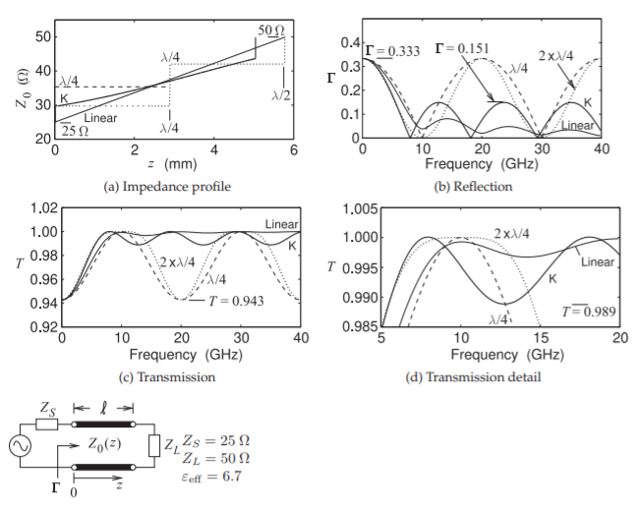
Figure \(\PageIndex{2}\): Characteristics of simulated transmission line transformers. Midband wavelength \(\lambda_{m} = 11.58\text{ mm}\) at \(f_{0} = 10\text{ GHz}\). Linear: Linear taper, \(\ell = \lambda_{m}/2\). \(\lambda/4\): \(\lambda/4\) transformer, \(\ell = \lambda_{m}/4\). \(2x\lambda /4\): two-section \(\lambda/4\) transformer, \(\ell = \lambda_{m}/2\). \(\text{K}\): Klopfenstein taper, \(\ell = 3.88\text{ mm} = 0.335\lambda_{m}\).
The Klopfenstein taper has the distinct advantage that the passband extends indefinitely above \(f_{\text{min}}\) where as one-stage and multi-stage quarter-wave transformers have a finite bandwidth.
The previous paragraph considered matching when \(Z_{L}/Z_{S} = 2\). A similar comparison is shown in Figure \(\PageIndex{3}\) for a much higher source and load impedance discontinuity with \(Z_{S} =5\:\Omega\) and \(Z_{L} = 50\:\Omega\) and the results are applicable in general for \(Z_{L}/Z_{S} = 10\). Figure \(\PageIndex{3}\)(a) shows the \(Z_{0}\) profile for the transmission line transformers and where the length of the linear taper has been chosen to provide comparable passband responses defined as where the transmission loss is less than \(0.1\text{ dB}\) (corresponding to a maximum reflection coefficient magnitude of \(0.151\)). The reflection coefficient response is shown in Figure \(\PageIndex{3}\)(b). First consider the responses of the single- and two-section quarter-wave transformers. Both provide an ideal match at the passband center frequency \(f_{0} = 10\text{ GHz}\) and repeating at odd multiples of \(f_{0}\).
Again the passband defined by the two-section quarter-wave transformer is used to determine the length of the linear and Klopfenstein tapers resulting in the linear taper being \(3\lambda_{m}\) long and the Klopfenstein taper being \(0.595\lambda_{m}\) long, slightly longer than the two-section quarter-wave transformer. The linear taper, chosen here to be \(\lambda_{m}/2\) long where \(\lambda_{m}\) is the guide wavelength at \(f_{0}\), has a reflection coefficient mismatch that reduces as frequency increases
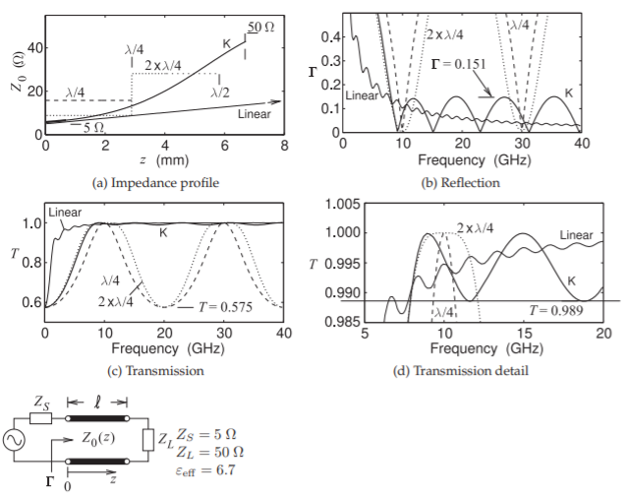
Figure \(\PageIndex{3}\): Characteristics of simulated transmission line transformers. Midband wavelength \(\lambda_{m} = 11.58\text{ mm}\) at \(f_{0} = 10\text{ GHz}\). Linear: Linear taper, \(\ell = \lambda_{m}/2\). \(\lambda/4\): \(\lambda/4\) transformer, \(\ell = \lambda_{m}/4\). \(2x\lambda/4\): two-section \(\lambda/4\) transformer, \(\ell = \lambda_{m}/2\). \(K\): Klopfenstein taper, \(\ell = 3.88\text{ mm} = 0.335\lambda_{m}\).
| \(Z_{L}/Z_{S}=2\) | \(\ell\) | Passband | Bandwidth |
|---|---|---|---|
| Linear taper | \(0.5\lambda_{m}\) | \(>6.53\text{ GHz}\) | |
| \(\lambda/4\) | \(0.25\lambda_{m}\) | \(7.16-11.84\text{ GHz}\) | \(50\%\) |
| \(2\times\lambda/4\) | \(0.5\lambda_{m}\) | \(5.43-14.57\text{ GHz}\) | \(91\%\) |
| Klopfenstein taper | \(0.335\lambda_{m}\) | \(>5.43\text{ GHz}\) | |
| \(Z_{L}/Z_{S}=10\) | |||
| Linear taper | \(3\lambda_{m}\) | \(>7.72\text{ GHz}\) | |
| \(\lambda/4\) | \(0.25\lambda_{m}\) | \(9.32-10.69\text{ GHz}\) | \(14\%\) |
| \(2\times\lambda/4\) | \(0.5\lambda_{m}\) | \(7.87-12.12\text{ GHz}\) | \(42\%\) |
| Klopfenstein taper | \(0.595\lambda_{m}\) | \(>7.87\text{ GHz}\) | |
| Exponential taper | \(1.68\lambda_{m}\) | \(>7.87\text{ GHz}\) | |
Table \(\PageIndex{3}\): Comparison of passbands of the four transmission line impedance transformers considered in Section 7.5.6 with \(\lambda_{m}\) being the guide wavelength at \(10\text{ GHz}\). The lengths of the tapers were chosen to have the same minimum passband frequency as the two-section quarter-wave transformer.
as the line becomes electrically longer.
The Klopfenstein taper for \(\Gamma_{m} = 0.151\) and \(Z_{L}/Z_{S} = 10\) has \(A = 2.720\) so that the passband of the Klopfenstein taper extends indefinitely above an electrical length of \(2.720\) radians and so choosing the minimum passband frequency \(f_{\text{min}}\) determines the physical length of the line.
The \(0.1\text{ dB}\) passbands of the transmission line transformers are compared in Table \(\PageIndex{3}\). The two-section quarter-wave transformer and the Klopfenstein transformer have comparable performance near the center frequency of the design with the choice being made on whether it is more important to have good transmission properties indefinitely above \(f_{\text{min}}\) or to provide some frequency selectivity by having a poorer match at the second harmonic frequency of the center match frequency, here \(f_{0}\).
7.5.7 Summary
The transmission line transformers considered in this section match resistive source and load impedances. However these impedance transformers provide guidance for design strategies when the source and load include reactances. When the source and load are resistances then the clear choice for a transmission-line-based impedance transformer is the Klopfenstein tape. With a reactive load the challenge is achieving broadband match since of course the reactance of the load and/or load will vary with frequency and so impose an overall bandwidth constraint. Design of the matching network needs to take into account the frequency characteristic of the load.
Different loads will have different frequency characteristics and hence variations in the type of matching network required. Four basic loads that are commonly encountered in microwave engineering and to which matching is required include the series RC model of the input of a FET transistor with a series reactance that is inversely proportional to frequency; the series LR model encountered in bonding to the input of a device where the inductance comes from a bond wire and which has a series reactance that is proportional to frequency; and a parallel RC load encountered at the output of a transistor with a susceptance that reduces with frequency. These two-element models of sources and loads are simple and other parasitics may need to be included. At microwave frequencies the \(Q\) of the impedances encountered with active devices is typically in the range of \(0.5\) to \(3\), and source/load resistance mismatch typically ranges from \(1.5\) to \(10\). For example, high mismatches are encountered at the output of power amplifiers.