
3.5: Microstrip Transmission Lines
- Page ID
- 41029

Transmission lines with conductors embedded in an inhomogeneous dielectric medium cannot support a pure TEM mode. This is the case even if the conductors are lossless. The most important member of this class is the microstrip transmission line (Figure 3.3.1(c)). Part of the field is in the air and part in the dielectric between the strip conductor and the ground. In most practical cases, the dielectric substrate is electrically thin, that is, \(h ≪\lambda\). Then the transverse field is dominant and the fields are called quasi-TEM.
The original analysis of microstrip was based on the unfolding of a coaxial line [13].
3.5.1 Microstrip Line in the Quasi-TEM Approximation
In this section a number of relations are developed based on the principle that the phase velocity of an EM wave in an air-only homogeneous transmission with a TEM field line is just \(c\). It is also shown that the static solutions for the transverse electric field alone can be used to calculate the characteristics of a transmission line. The procedure described is used in many EM computer programs to calculate the characteristics of transmission lines.
As a first step, the potential of the conductor strip is set to \(V_{0}\) and Laplace’s equation is solved using an EM simulator for the electrostatic potential everywhere in the dielectric. Then the per unit length (p.u.l.) electric charge, \(Q\), on the conductor is determined. Using this in the following relation gives the line capacitance:
\[C=\frac{Q}{V_{0}}\nonumber \]
In the next step, the process is repeated with \(\varepsilon_{r} = 1\) to determine \(C_{\text{air}}\) (the capacitance of the line without a dielectric).
If the microstrip line is now an air-filled lossless TEM structure,
\[\label{eq:1}v_{p,\text{ air}}=c=\frac{1}{LC_{\text{air}}} \]
and so
\[\label{eq:2}L=\frac{1}{c^{2}C_{\text{air}}} \]
\(L\) is not affected by the dielectric properties of the medium.\(^{1}\) \(L\) calculated above is the desired p.u.l. inductance of the line with the dielectric as well as in free space. Once \(L\) and \(C\) have been found, the characteristic impedance can be found using
\[\label{eq:3}Z_{0}=\sqrt{\frac{L}{C}} \]
rewritten as
\[\label{eq:4}Z_{0}=\frac{1}{c}\frac{1}{\sqrt{CC_{\text{air}}}} \]
and the phase velocity is
\[\label{eq:5}v_{p}=\frac{1}{\sqrt{LC}}=c\sqrt{\frac{C_{\text{air}}}{C}} \]
Now the field is distributed in the inhomogeneous medium and in free space, as shown in Figure \(\PageIndex{1}\)(a). So the effective relative permittivity, \(\varepsilon_{e}\), of the equivalent homogeneous microstrip line (see Figure \(\PageIndex{1}\)(b)) is defined by
\[\label{eq:6}\sqrt{\varepsilon_{e}}=\frac{c}{v_{p}} \]
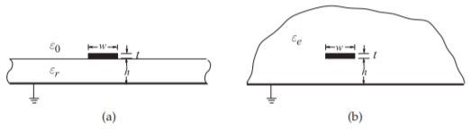
Figure \(\PageIndex{1}\): Microstrip /ink.sh micr (a) cross section; and (b) approximate equivalent structure where the strip is embedded in a dielectric of semi-infinite extent with effective relative permittivity \(\varepsilon_{e}\).
Combining Equations \(\eqref{eq:5}\) and \(\eqref{eq:6}\), the effective relative permittivity (usually just the term effective permittivity is used) is obtained:
\[\label{eq:7}\varepsilon_{e}=\frac{C}{C_{\text{air}}} \]
The effective permittivity can be interpreted as the permittivity of a homogeneous medium that replaces the air and the dielectric regions of the microstrip, as shown in Figure \(\PageIndex{1}\). Since some of the field is in the dielectric and some is in air, the effective relative permittivity must satisfy
\[\label{eq:8}1<\varepsilon_{e}<\varepsilon_{r} \]
However, the minimum \(\varepsilon_{e}\) will be greater than \(1\) as electrical energy will be distributed in air and dielectric. The wavelength on a transmission line, the guide wavelength \(\lambda_{g}\), is related to the free space wavelength by \(\lambda_{g} =\lambda_{0}/\sqrt{\varepsilon_{e}}\).
A microstrip line has a characteristic impedance \(Z_{0}\) of \(50\:\Omega\) derived from reflection coefficient measurements and an effective permittivity, \(\varepsilon_{e}\), of \(7\) derived from measurement of phase velocity. What is the line’s per-unit-length inductance, \(L\), and capacitance, \(C\)?
Solution
The key equations are \(Z_{0} =\sqrt{L/C},\: \varepsilon_{e} = C/C_{\text{air}}\), and for the air-filled microstrip line (with a TEM mode) \(v_{p} = 1/\sqrt{LC_{\text{air}}} = c\). Also assume that \(\mu_{r} = 1\) which is the default if not specified otherwise and also that \(L\) does not change if only the dielectric is changed. Thus
\[C_{\text{air}}=\frac{C}{\varepsilon_{e}}\quad\text{and then}\quad L=\frac{\varepsilon_{e}}{c^{2}C}\quad\text{so that}\quad Z_{0}=\sqrt{\frac{L}{C}}=\frac{\sqrt{\varepsilon_{e}}}{cC},\quad\text{that is}\quad C=\frac{\sqrt{\varepsilon_{e}}}{cZ_{0}}\nonumber \]
So \(C =\sqrt{7}/(2.998\cdot 10^{8}\times 50) = 1.765\cdot 10^{−10} = 176.5\text{ pF/m}\) and \(L = Z_{0}^{2} C = 441.3\text{ nH/m}\).
3.5.2 Input Impedance of a Shorted Microstrip Line Modeled using a Field Solver
In this example a shorted microstrip line is examined with the aid of a microwave computer-aided design tool. The specific tool used here is National Instruments AWR Design Environment (AWRDE), but most microwave analysis tools will provide the same insight. The project file for the AWR Design Environment is RFDesign Shorted Microstrip Line.emp.
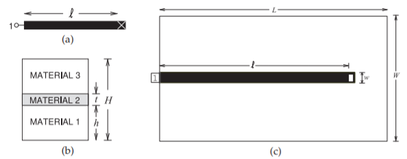
Figure \(\PageIndex{2}\): Microstrip line layout: (a) microstrip schematic; (b) stack-up of materials with material \(1\) being the substrate, material \(2\) being the metal of the strip, and Material \(3\) being vacuum; and (c) simulation layout. Dimensions are \(w = 500\:\mu\text{m},\:\ell = 1\text{ cm}\). The metal is \(t = 6\:\mu\text{m}\) thick gold (conductivity \(\sigma = 42.6\times 10^{6}\text{ S/m}\)) and the alumina substrate height is \(h = 600\:\mu\text{m}\) with relative permittivity \(\varepsilon_{r} = 9.8\) and loss tangent \(0.001\). The size of the simulation box is defined by \(W = 6\text{ mm},\: L = 12\text{ mm}\), and box height \(H = 2.61\text{ mm}\).
The schematic of the microstrip line is shown in Figure \(\PageIndex{2}\)(a). This is what the microstrip looks like from above, with the black region indicating metal and the white cross indicating a via that connects the strip to the ground plane. The distance from the start of the line to the wall of the via is \(\ell\). The via has a finite length and it is important to take the length of the line up to the wall that terminates the propagating electric and magnetic fields of the microstrip line and not to the center point of the via. While vias are typically cylinders, and so there is not an electric wall across the microstrip, the part of the wall of the via that first encounters the EM fields guided by the microstrip line is a good approximation.
To perform an EM analysis of this line it is necessary to define an enclosure with the cross section shown in Figure \(\PageIndex{2}\)(b) and the top view shown in Figure \(\PageIndex{2}\)(c). The enclosure sets up the walls that terminate the EM field lines. Here the enclosure is a metal box length \(L = 12\text{ mm}\) and width \(W = 6\text{ mm}\). The height of the enclosure depends on the thicknesses assigned to the three materials that comprise the microstrip environment (see Figure \(\PageIndex{2}\)(b)). The enclosure here is a metal box, but options are usually provided to define walls as electric or magnetic walls, and in addition the top walls of the box can be defined as absorbing walls. An absorbing or free-space wall presents an approximation to the free-space conditions. In this example six electric walls are used, with the side walls and top wall spaced a good distance from the line so that the fields are not perturbed by the presence of the side walls.
There are two main types of frequency-domain EM solvers used in microwave engineering. One type uses the finite element method (FEM), which solves for the fields at every grid point in a three-dimensional volume. This can provide a wealth of information and handle a broad range of microwave structures. However, it is very slow and runs into memory problems for all but the simplest structures. The other type of solver is called
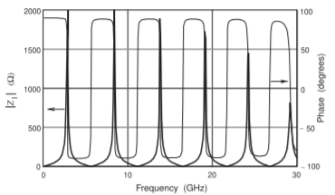
Figure \(\PageIndex{3}\): Magnitude and phase of the input impedance, \(Z_{1}\), of the microstrip line in Figure \(\PageIndex{2}\).
a two-and-a-half dimensional (or \(2\frac{1}{2}\)D) field solver. This type of solver uses what is called the method of moments to solve for the charges on the surfaces of metals. Fields are not found at every point in space and so a \(2\frac{1}{2}\)D field solver is much faster than a \(3\)D solver. The type of solver that will be used here is a \(2\frac{1}{2}\)D field solver available in the AWRDE environment and also used in the Sonnet simulations used elsewhere in this book. The restriction that comes with using a \(2\frac{1}{2}\)D field solver is that the conductors and dielectrics must be arranged in layers, as shown in Figure \(\PageIndex{2}\)(b). Metals are treated as infinitely thin and, in some tools, dielectrics can be arranged as blocks, but still following the layering protocol.
The layout in the horizontal \(x-y\) plane in Figure \(\PageIndex{2}\)(c) is very close to the schematic view shown in Figure \(\PageIndex{2}\)(a). Port \(\mathsf{1}\) (the only port) of the microstrip line is shown on the left in Figure \(\PageIndex{2}\)(a) and in Figure \(\PageIndex{2}\)(c) it is embedded in the left electric wall. As was mentioned, a \(2\frac{1}{2}\)D field solver finds the charges on the metal. A grid of cells is established and most often the grid is a regular rectangular mesh and curves and oblique angles can only be approximated. Even when more sophisticated meshes are used, a curved shape is approximated by straight lines. In Figure \(\PageIndex{2}\)(c) the via is inserted as a rectangular cuboid. Another restriction of \(2\frac{1}{2}\)D field solvers is that currents must flow either in the \(x-y\) plane or in the vertical (\(z\)) direction. So as long as the via has a small (relative to a wavelength) dimension in the \(z\) direction and the \(x-y\) dimensions of the via are small, this is a small restriction in exchange for a simulation that can be thousands of times faster than full \(3\)D methods.
The dimensions of the microstrip were chosen for a characteristic impedance of \(50\:\Omega\) yielding \(w = 500\:\mu\text{m}\) for the alumina dielectric with relative permittivity \(\varepsilon_{r} = 9.8\) and height \(h = 600\:\mu\text{m}\). Also \(\ell = 1\text{ cm}\). Often it is necessary to include realistic loss for the materials to obtain physically meaningful results. Here the metal of the line and of the bottom wall is gold with conductivity \(\sigma = 42.6\times 10^{6}\text{ S/m}\) and the loss tangent of the alumina is \(0.001\). The strip has a thickness \(t = 6\:\mu\text{m}\). The metal strip is simulated as though it was infinitely thin, but the thickness is used in calculating the resistance of the strip. The dielectric above the strip is free space with permittivity \(\varepsilon_{0}\) and with a thickness of \(2\text{ mm}\). So the height of the box \(H = h + t + 2\text{ mm} = 2.610\text{ mm}\).
The input impedance, \(Z_{\text{in}}\), of the shorted microstrip line is shown in Figure \(\PageIndex{3}\). The plots show the magnitude and phase of the input impedance. The phase is mostly \(+90^{\circ}\) or \(−90^{\circ}\), indicating that \(Z_{\text{in}}\) is mostly reactive. At low frequencies near \(0\text{ GHz}\), the input impedance is inductive since
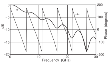
Figure \(\PageIndex{4}\): Magnitude and phase of the input reflection coefficient, \(\Gamma\), of the microstrip line in Figure \(\PageIndex{2}\) but now with a high loss substrate with \(\tan\delta = 0.1\).
the phase is approximately \(+90^{\circ}\). \(Z_{\text{in}}\) increases as would be expected from the approximate model of a shorted line. At \(3\text{ GHz}\), \(Z_{\text{in}}\) changes from inductive to capacitive going through a near-open circuit. The transition is not instantaneous, as the line is lossy. \(Z_{\text{in}}\) continues to cycle as the excitation frequency increases.
It is interesting to view what happens when the loss is greatly increased. Here this is done by increasing the loss tangent of the dielectric, \(\tan\delta\), to \(0.1\). This is much higher than that of any useful substrate. The reflection coefficient of the high loss line is shown in Figure \(\PageIndex{4}\). At very low frequencies \(|\Gamma|\approx 0\text{ dB}\), i.e., \(|\Gamma|\approx 1\). The phase of \(\Gamma\approx 180^{\circ}\) so that \(\Gamma\approx −1\) (i.e., a short circuit). As frequency increases \(|\Gamma|\) decreases because of increasing dielectric loss and the phase of \(\Gamma\) monotonically decreases as the line becomes electrically longer.
3.5.3 Effective Permittivity and Characteristic Impedance
This section presents formulas for the effective permittivity and characteristic impedance of a microstrip line. These formulas are fits to the results of detailed EM simulations. Also, the form of the equations is based on good physical understanding. First, assume that the thickness, \(t\), is zero. This is not a bad approximation, as \(t ≪ w, h\) for most microwave circuits.
Hammerstad and others provide well-accepted formulas for calculating the effective permittivity and characteristic impedance of microstrip lines [14, 15, 16]. Given \(\varepsilon_{r},\: w,\) and \(h\), the effective relative permittivity is
Mostly the term “effective permittivity” is used to mean effective relative permittivity (check the magnitude).
\[\label{eq:9}\varepsilon_{e}=\frac{\varepsilon_{r}+1}{2}+\frac{\varepsilon_{r}-1}{2}\left(1+\frac{10h}{w}\right)^{-a\cdot b} \]
where
\[\label{eq:10} a(u)|_{u=w/h}=1+\frac{1}{49}\ln\left[\frac{u^{4}+\{u/52\}^{2}}{u^{4}+0.432}\right]+\frac{1}{18.7}\ln\left[1+\left(\frac{u}{18.1}\right)^{3}\right] \]
and
\[\label{eq:11}b(\varepsilon_{r})=0.564\left[\frac{\varepsilon_{r}-0.9}{\varepsilon_{r}+3}\right]^{0.053} \]
Take some time to interpret Equation \(\eqref{eq:9}\), the formula for effective relative permittivity. If \(\varepsilon_{r} = 1\), then \(\varepsilon_{e} = (1 + 1)/2+0 = 1\), as expected. If \(\varepsilon_{r}\) is not that of air, then \(\varepsilon_{e}\) will be between \(1\) and \(\varepsilon_{r}\), dependent on the geometry of the line, or more specifically, the ratio \(w/h\). For a very wide line, \(w/h ≫ 1\), \(\varepsilon_{e} = (\varepsilon_{r} + 1)/2+(\varepsilon_{r} − 1)/2 = \varepsilon_{r}\), corresponding to the EM energy being confined to the dielectric. For a thin line \(w/h ≪ 1\), \(\varepsilon_{e} = (\varepsilon_{r} + 1)/2\), the average of the dielectric and air permittivities.
The characteristic impedance is given by
\[\label{eq:12}Z_{0}=\frac{Z_{01}}{\sqrt{\varepsilon_{e}}} \]
where the characteristic impedance of the microstrip line in free space is
\[\label{eq:13}Z_{01}=Z_{0}|_{(\varepsilon_{r}=1)}=60\ln\left[\frac{F_{1}h}{w}+\sqrt{1+\left(\frac{2h}{w}\right)^{2}}\right] \]
and
\[\label{eq:14}F_{1}=6+(2\pi -6)\exp\left\{-(30.666h/w)^{0.7528}\right\} \]
The accuracy of Equation \(\eqref{eq:9}\) is better than \(0.2\%\) for \(0.01 ≤ w/h ≤ 100\) and \(1 ≤\varepsilon_{r} ≤ 128\). Also, the accuracy of Equation \(\eqref{eq:13}\) is better than \(0.1\%\) for \(w/h < 1000\). Note that \(Z_{0}\) has a maximum value when \(w\) is small.
Now consider the special case where \(w\) is vanishingly small. Then εe has its minimum value:
\[\label{eq:15}\varepsilon_{e}=\frac{1}{2}(\varepsilon_{r}+1) \]
This leads to an approximate (and convenient) form of Equation \(\eqref{eq:9}\):
\[\label{eq:16} \varepsilon_{e}=\frac{(\varepsilon_{r}+1)}{2}+\frac{(\varepsilon_{r}-1)}{2}\frac{1}{\sqrt{1+12h/w}} \]
This approximation has its greatest error of \(1\%\) for low and high \(\varepsilon_{r}\) and narrow lines, \(w/h ≪ 1\). Again, Equation \(\eqref{eq:12}\) is used to calculate the characteristic impedance. A comparison of the line characteristics using the more precise formula for εe (Equation \(\eqref{eq:9}\)) and the slightly less accurate fit (Equation \(\eqref{eq:16}\)) is given in Table \(\PageIndex{1}\).
The more exact analysis, represented by Equation \(\eqref{eq:9}\), was used to develop Table \(\PageIndex{2}\), which can be used in the design of microstrip on a silicon dioxide (SiO\(_{2}\)) substrate and on an FR4 printed circuit board that both have a relative permittivity of \(4\), on alumina with a permittivity of \(10\), on a silicon (Si) substrate with a relative permittivity of \(11.9\), and on a gallium arsenide (GaAs) substrate with a relative permittivity of \(12.85\).
The strip of a microstrip line has a width of \(600\:\mu\text{m}\) and is fabricated on a lossless substrate that is \(635\:\mu\text{m}\) thick and has a relative permittivity of \(4.1\).
- What is the effective relative permittivity?
- What is the characteristic impedance?
- What is the propagation constant at \(5\text{ GHz}\) ignoring any losses?
Solution
Use the formulas for effective permittivity, characteristic impedance, and attenuation constant from Section 3.5.3 with \(w = 600\:\mu\text{m};\: h = 635\:\mu\text{m};\:\varepsilon_{r} = 4.1;\: w/h = 600/635 = 0.945\).
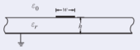
Figure \(\PageIndex{5}\)
-
\[\varepsilon_{e}=\frac{\varepsilon_{r}+1}{2}+\frac{\varepsilon_{r}-1}{2}\left(1+\frac{10h}{w}\right)^{-a\cdot b}\nonumber \]
From Equations \(\eqref{eq:10}\) and \(\eqref{eq:11}\),
\[\begin{aligned}a&=1+\frac{1}{49}\ln\left[\frac{(w/h)^{4}+\{w/(52h)\}^{2}}{(w/h)^{4}+0.432}\right]+\frac{1}{18.7}\ln\left[1+\left(\frac{w}{18.1h}\right)^{3}\right]=0.991 \\ b&=0.564\left[\frac{\varepsilon_{r}-0.9}{\varepsilon_{r}+3}\right]^{0.053}=0.541\nonumber\end{aligned} \nonumber \]
From Equation \(\eqref{eq:9}\), \(\varepsilon_{e} = 2.967\). - In free space,
\[Z_{0}|_{\text{air}}=60\ln\left[\frac{F_{1}\cdot h}{w}+\sqrt{1+\left(\frac{2h}{w}\right)^{2}}\right]\nonumber \]
where \(F_{1} = 6 + (2π − 6) \exp\left\{ − (30.666h/\omega ) ^{0.7528}\right\} ,\quad Z_{0} = Z_{0}|_{\text{air}}/\sqrt{\varepsilon_{e}}\)
\[Z_{0}|_{\text{air}}=129.7\:\Omega\quad\text{and}\quad Z_{0}=Z_{0}|_{\text{air}}/\sqrt{\varepsilon_{e}}=75.3\:\Omega\nonumber \] - \(f=5\text{ GHz}\), \(\omega =2\pi f\), \(\gamma=\jmath\omega\sqrt{\mu_{0}\varepsilon_{0}\varepsilon_{e}}=\jmath 180.5/\text{ m}\)
| \(\varepsilon_{r}\) | \(w/h\) | \(\varepsilon_{e}\) | \(Z_{0}\) | \(\varepsilon_{e}\) | \(Z_{0}\) |
|---|---|---|---|---|---|
| Eq. \(\eqref{eq:9}\), \(0.2\%\) | Eq. \(\eqref{eq:16}\), \(1\%\) | ||||
| \(1\) | \(0.01\) | \(1\) | \(401.1\) | \(1\) | \(401.1\) |
| \(1\) | \(0.1\) | \(1\) | \(262.9\) | \(1\) | \(262.9\) |
| \(1\) | \(1\) | \(1\) | \(126.5\) | \(1\) | \(126.5\) |
| \(1\) | \(10\) | \(1\) | \(29.04\) | \(1\) | \(29.04\) |
| \(1\) | \(100\) | \(1\) | \(3.61\) | \(1\) | \(3.61\) |
| \(2\) | \(0.01\) | \(1.525\) | \(322.5\) | \(1.514\) | \(325.9\) |
| \(2\) | \(0.1\) | \(1.565\) | \(210.0\) | \(1.545\) | \(211.5\) |
| \(2\) | \(1\) | \(1.645\) | \(98.64\) | \(1.639\) | \(98.83\) |
| \(2\) | \(10\) | \(1.848\) | \(21.36\) | \(1.837\) | \(21.43\) |
| \(2\) | \(100\) | \(1.969\) | \(2.58\) | \(1.972\) | \(2.58\) |
| \(10\) | \(0.01\) | \(5.683\) | \(165.8\) | \(5.630\) | \(169.0\) |
| \(10\) | \(0.1\) | \(6.016\) | \(107.0\) | \(5.909\) | \(108.2\) |
| \(10\) | \(1\) | \(6.705\) | \(48.86\) | \(6.748\) | \(48.70\) |
| \(10\) | \(10\) | \(8.556\) | \(9.93\) | \(8.534\) | \(9.94\) |
| \(10\) | \(100\) | \(9.707\) | \(1.16\) | \(9.752\) | \(1.16\) |
| \(20\) | \(0.01\) | \(10.88\) | \(119.6\) | \(10.77\) | \(122.2\) |
| \(20\) | \(0.1\) | \(11.57\) | \(77.14\) | \(11.36\) | \(78.00\) |
| \(20\) | \(1\) | \(13.01\) | \(35.07\) | \(13.13\) | \(34.91\) |
| \(20\) | \(10\) | \(16.93\) | \(7.06\) | \(16.91\) | \(7.06\) |
| \(20\) | \(100\) | \(19.38\) | \(0.821\) | \(19.48\) | \(0.819\) |
| \(128\) | \(0.01\) | \(66.90\) | \(48.15\) | \(66.30\) | \(49.25\) |
| \(128\) | \(0.1\) | \(71.51\) | \(31.02\) | \(70.27\) | \(31.37\) |
| \(128\) | \(1\) | \(81.12\) | \(14.05\) | \(82.11\) | \(13.96\) |
| \(128\) | \(10\) | \(71.51\) | \(2.80\) | \(70.27\) | \(2.80\) |
| \(128\) | \(100\) | \(123.8\) | \(0.325\) | \(124.5\) | \(0.324\) |
Table \(\PageIndex{1}\): Comparison of two fitted equations for the effective relative permittivity and characteristic impedance of a microstrip line. Equation \(\eqref{eq:9}\) has an accuracy of better than \(0.2\%\) and Equation \(\eqref{eq:16}\) has an accuracy of better than \(1\%\).
| \(Z_{0}\) | \(\varepsilon_{r} =4\text{ (SiO}_{2}\text{, FR4)}\) | \(\varepsilon_{r}=10\:\text{(Alumina)}\) | \(\varepsilon_{r}=11.9\:\text{(Si)}\) | |||
|---|---|---|---|---|---|---|
| (\(\Omega \)) | \(u\) | \(\varepsilon_{e}\) | \(u\) | \(\varepsilon_{e}\) | \(u\) | \(\varepsilon_{e}\) |
| \(140\) | \(0.171\) | \(2.718\) | \(0.028\) | \(5.914\) | \(0.017\) | \(6.907\) |
| \(139\) | \(0.176\) | \(2.720\) | \(0.029\) | \(5.917\) | \(0.018\) | \(6.910\) |
| \(138\) | \(0.181\) | \(2.722\) | \(0.030\) | \(5.919\) | \(0.019\) | \(6.914\) |
| \(137\) | \(0.185\) | \(2.723\) | \(0.031\) | \(5.922\) | \(0.020\) | \(6.919\) |
| \(136\) | \(0.190\) | \(2.725\) | \(0.032\) | \(5.924\) | \(0.021\) | \(6.923\) |
| \(135\) | \(0.195\) | \(2.727\) | \(0.033\) | \(5.927\) | \(0.022\) | \(6.925\) |
| \(134\) | \(0.201\) | \(2.729\) | \(0.035\) | \(5.931\) | \(0.022\) | \(6.927\) |
| \(133\) | \(0.206\) | \(2.731\) | \(0.036\) | \(5.933\) | \(0.023\) | \(6.930\) |
| \(132\) | \(0.212\) | \(2.733\) | \(0.037\) | \(5.936\) | \(0.024\) | \(6.934\) |
| \(131\) | \(0.217\) | \(2.734\) | \(0.038\) | \(5.939\) | \(0.025\) | \(6.937\) |
| \(130\) | \(0.223\) | \(2.736\) | \(0.040\) | \(5.942\) | \(0.026\) | \(6.941\) |
| \(129\) | \(0.229\) | \(2.738\) | \(0.043\) | \(5.949\) | \(0.028\) | \(6.948\) |
| \(128\) | \(0.235\) | \(2.740\) | \(0.044\) | \(5.951\) | \(0.029\) | \(6.951\) |
| \(127\) | \(0.241\) | \(2.742\) | \(0.046\) | \(5.955\) | \(0.030\) | \(6.954\) |
| \(126\) | \(0.248\) | \(2.744\) | \(0.048\) | \(5.958\) | \(0.031\) | \(6.957\) |
| \(125\) | \(0.254\) | \(2.746\) | \(0.050\) | \(5.962\) | \(0.033\) | \(6.963\) |
| \(124\) | \(0.261\) | \(2.748\) | \(0.052\) | \(5.966\) | \(0.034\) | \(6.966\) |
| \(123\) | \(0.268\) | \(2.750\) | \(0.054\) | \(5.970\) | \(0.035\) | \(6.969\) |
| \(122\) | \(0.275\) | \(2.752\) | \(0.056\) | \(5.973\) | \(0.038\) | \(6.977\) |
| \(121\) | \(0.283\) | \(2.755\) | \(0.058\) | \(5.977\) | \(0.039\) | \(6.980\) |
| \(120\) | \(0.290\) | \(2.757\) | \(0.061\) | \(5.982\) | \(0.041\) | \(6.985\) |
| \(119\) | \(0.298\) | \(2.759\) | \(0.063\) | \(5.985\) | \(0.043\) | \(6.990\) |
| \(118\) | \(0.306\) | \(2.761\) | \(0.066\) | \(5.990\) | \(0.045\) | \(6.995\) |
| \(117\) | \(0.314\) | \(2.763\) | \(0.068\) | \(5.993\) | \(0.047\) | \(6.999\) |
| \(116\) | \(0.323\) | \(2.766\) | \(0.071\) | \(5.998\) | \(0.049\) | \(7.004\) |
| \(115\) | \(0.331\) | \(2.768\) | \(0.074\) | \(6.003\) | \(0.051\) | \(7.008\) |
| \(114\) | \(0.340\) | \(2.771\) | \(0.077\) | \(6.007\) | \(0.053\) | \(7.013\) |
| \(113\) | \(0.349\) | \(2.773\) | \(0.080\) | \(6.012\) | \(0.055\) | \(7.017\) |
| \(112\) | \(0.359\) | \(2.776\) | \(0.083\) | \(6.016\) | \(0.057\) | \(7.022\) |
| \(111\) | \(0.368\) | \(2.778\) | \(0.086\) | \(6.021\) | \(0.060\) | \(7.028\) |
| \(110\) | \(0.378\) | \(2.781\) | \(0.089\) | \(6.025\) | \(0.062\) | \(7.032\) |
| \(109\) | \(0.389\) | \(2.783\) | \(0.093\) | \(6.031\) | \(0.065\) | \(7.038\) |
| \(108\) | \(0.399\) | \(2.786\) | \(0.097\) | \(6.036\) | \(0.068\) | \(7.044\) |
| \(107\) | \(0.410\) | \(2.789\) | \(0.100\) | \(6.040\) | \(0.071\) | \(7.050\) |
| \(106\) | \(0.421\) | \(2.791\) | \(0.104\) | \(6.046\) | \(0.074\) | \(7.055\) |
| \(105\) | \(0.432\) | \(2.794\) | \(0.109\) | \(6.052\) | \(0.077\) | \(7.061\) |
| \(104\) | \(0.444\) | \(2.797\) | \(0.113\) | \(6.057\) | \(0.080\) | \(7.066\) |
| \(103\) | \(0.456\) | \(2.800\) | \(0.117\) | \(6.062\) | \(0.084\) | \(7.073\) |
| \(102\) | \(0.468\) | \(2.803\) | \(0.122\) | \(6.069\) | \(0.087\) | \(7.079\) |
| \(101\) | \(0.481\) | \(2.806\) | \(0.127\) | \(6.075\) | \(0.091\) | \(7.085\) |
| \(100\) | \(0.494\) | \(2.809\) | \(0.132\) | \(6.081\) | \(0.095\) | \(7.092\) |
| \(99\) | \(0.507\) | \(2.812\) | \(0.137\) | \(6.087\) | \(0.099\) | \(7.099\) |
| \(98\) | \(0.521\) | \(2.815\) | \(0.143\) | \(6.094\) | \(0.103\) | \(7.105\) |
| \(97\) | \(0.535\) | \(2.819\) | \(0.148\) | \(6.100\) | \(0.108\) | \(7.113\) |
| \(96\) | \(0.550\) | \(2.822\) | \(0.154\) | \(6.106\) | \(0.112\) | \(7.120\) |
| \(95\) | \(0.565\) | \(2.825\) | \(0.160\) | \(6.113\) | \(0.117\) | \(7.127\) |
| \(94\) | \(0.580\) | \(2.829\) | \(0.167\) | \(6.121\) | \(0.122\) | \(7.135\) |
| \(93\) | \(0.596\) | \(2.832\) | \(0.173\) | \(6.127\) | \(0.128\) | \(7.144\) |
| \(92\) | \(0.612\) | \(2.836\) | \(0.180\) | \(6.134\) | \(0.133\) | \(7.151\) |
| \(91\) | \(0.629\) | \(2.839\) | \(0.187\) | \(6.142\) | \(0.139\) | \(7.159\) |
| \(90\) | \(0.646\) | \(2.843\) | \(0.195\) | \(6.150\) | \(0.145\) | \(7.168\) |
| \(89\) | \(0.664\) | \(2.847\) | \(0.202\) | \(6.157\) | \(0.151\) | \(7.176\) |
| \(87\) | \(0.701\) | \(2.855\) | \(0.219\) | \(6.173\) | \(0.164\) | \(7.193\) |
| \(86\) | \(0.721\) | \(2.859\) | \(0.228\) | \(6.182\) | \(0.171\) | \(7.203\) |
| \(85\) | \(0.740\) | \(2.863\) | \(0.237\) | \(6.190\) | \(0.179\) | \(7.213\) |
| \(84\) | \(0.761\) | \(2.867\) | \(0.246\) | \(6.198\) | \(0.187\) | \(7.223\) |
| \(83\) | \(0.782\) | \(2.872\) | \(0.256\) | \(6.208\) | \(0.195\) | \(7.233\) |
| \(82\) | \(0.804\) | \(2.876\) | \(0.266\) | \(6.216\) | \(0.203\) | \(7.242\) |
| \(81\) | \(0.826\) | \(2.881\) | \(0.277\) | \(6.226\) | \(0.212\) | \(7.253\) |
| \(80\) | \(0.849\) | \(2.885\) | \(0.288\) | \(6.235\) | \(0.221\) | \(7.263\) |
| \(79\) | \(0.873\) | \(2.890\) | \(0.299\) | \(6.245\) | \(0.230\) | \(7.274\) |
| \(78\) | \(0.898\) | \(2.895\) | \(0.311\) | \(6.255\) | \(0.240\) | \(7.285\) |
| \(77\) | \(0.923\) | \(2.900\) | \(0.324\) | \(6.265\) | \(0.251\) | \(7.297\) |
| \(76\) | \(0.949\) | \(2.905\) | \(0.337\) | \(6.276\) | \(0.262\) | \(7.309\) |
| \(75\) | \(0.976\) | \(2.910\) | \(0.350\) | \(6.286\) | \(0.273\) | \(7.321\) |
| \(74\) | \(1.003\) | \(2.915\) | \(0.364\) | \(6.297\) | \(0.285\) | \(7.333\) |
| \(73\) | \(1.032\) | \(2.921\) | \(0.379\) | \(6.309\) | \(0.297\) | \(7.345\) |
| \(72\) | \(1.062\) | \(2.926\) | \(0.394\) | \(6.320\) | \(0.310\) | \(7.359\) |
| \(71\) | \(1.092\) | \(2.932\) | \(0.410\) | \(6.332\) | \(0.323\) | \(7.371\) |
| \(70\) | \(1.123\) | \(2.937\) | \(0.426\) | \(6.34\) | \(0.338\) | \(7.386\) |
| \(69\) | \(1.156\) | \(2.943\) | \(0.444\) | \(6.357\) | \(0.352\) | \(7.399\) |
| \(68\) | \(1.190\) | \(2.949\) | \(0.462\) | \(6.369\) | \(0.368\) | \(7.414\) |
| \(67\) | \(1.224\) | \(2.955\) | \(0.480\) | \(6.382\) | \(0.384\) | \(7.429\) |
| \(66\) | \(1.260\) | \(2.961\) | \(0.500\) | \(6.396\) | \(0.400\) | \(7.444\) |
| \(65\) | \(1.298\) | \(2.968\) | \(0.520\) | \(6.410\) | \(0.418\) | \(7.460\) |
| \(64\) | \(1.336\) | \(2.974\) | \(0.541\) | \(6.424\) | \(0.436\) | \(7.476\) |
| \(63\) | \(1.376\) | \(2.980\) | \(0.563\) | \(6.439\) | \(0.455\) | \(7.492\) |
| \(62\) | \(1.417\) | \(2.987\) | \(0.586\) | \(6.454\) | \(0.475\) | \(7.509\) |
| \(61\) | \(1.460\) | \(2.994\) | \(0.610\) | \(6.470\) | \(0.496\) | \(7.527\) |
| \(60\) | \(1.504\) | \(3.001\) | \(0.635\) | \(6.486\) | \(0.518\) | \(7.545\) |
| \(59\) | \(1.551\) | \(3.008\) | \(0.661\) | \(6.502\) | \(0.541\) | \(7.564\) |
| \(58\) | \(1.598\) | \(3.015\) | \(0.688\) | \(6.519\) | \(0.564\) | \(7.583\) |
| \(57\) | \(1.648\) | \(3.022\) | \(0.717\) | \(6.538\) | \(0.589\) | \(7.603\) |
| \(56\) | \(1.700\) | \(3.030\) | \(0.746\) | \(6.556\) | \(0.616\) | \(7.624\) |
| \(55\) | \(1.753\) | \(3.037\) | \(0.777\) | \(6.575\) | \(0.643\) | \(7.645\) |
| \(54\) | \(1.809\) | \(3.045\) | \(0.809\) | \(6.594\) | \(0.672\) | \(7.667\) |
| \(53\) | \(1.867\) | \(3.053\) | \(0.843\) | \(6.614\) | \(0.702\) | \(7.690\) |
| \(52\) | \(1.927\) | \(3.061\) | \(0.878\) | \(6.635\) | \(0.733\) | \(7.713\) |
| \(51\) | \(1.991\) | \(3.069\) | \(0.915\) | \(6.657\) | \(0.766\) | \(7.738\) |
| \(50\) | \(2.056\) | \(3.077\) | \(0.954\) | \(6.679\) | \(0.800\) | \(7.763\) |
| \(49\) | \(2.125\) | \(3.086\) | \(0.995\) | \(6.702\) | \(0.837\) | \(7.790\) |
| \(48\) | \(2.197\) | \(3.094\) | \(1.037\) | \(6.726\) | \(0.875\) | \(7.817\) |
| \(47\) | \(2.272\) | \(3.103\) | \(1.081\) | \(6.750\) | \(0.914\) | \(7.845\) |
| \(46\) | \(2.350\) | \(3.112\) | \(1.128\) | \(6.775\) | \(0.956\) | \(7.874\) |
| \(45\) | \(2.432\) | \(3.121\) | \(1.177\) | \(6.801\) | \(1.000\) | \(7.904\) |
| \(44\) | \(2.518\) | \(3.131\) | \(1.229\) | \(6.828\) | \(1.047\) | \(7.936\) |
| \(43\) | \(2.609\) | \(3.140\) | \(1.283\) | \(6.856\) | \(1.096\) | \(7.968\) |
| \(42\) | \(2.703\) | \(3.150\) | \(1.340\) | \(6.884\) | \(1.147\) | \(8.002\) |
| \(41\) | \(2.803\) | \(3.160\) | \(1.400\) | \(6.913\) | \(1.201\) | \(8.036\) |
| \(40\) | \(2.908\) | \(3.171\) | \(1.464\) | \(6.944\) | \(1.259\) | \(8.072\) |
| \(39\) | \(3.019\) | \(3.181\) | \(1.531\) | \(6.974\) | \(1.319\) | \(8.108\) |
| \(38\) | \(3.136\) | \(3.192\) | \(1.602\) | \(7.006\) | \(1.384\) | \(8.147\) |
| \(37\) | \(3.259\) | \(3.203\) | \(1.677\) | \(7.039\) | \(1.452\) | \(8.186\) |
| \(36\) | \(3.390\) | \(3.214\) | \(1.757\) | \(7.073\) | \(1.524\) | \(8.226\) |
| \(35\) | \(3.528\) | \(3.226\) | \(1.841\) | \(7.108\) | \(1.600\) | \(8.268\) |
| \(34\) | \(3.675\) | \(3.237\) | \(1.931\) | \(7.143\) | \(1.682\) | \(8.311\) |
| \(33\) | \(3.831\) | \(3.250\) | \(2.027\) | \(7.180\) | \(1.769\) | \(8.355\) |
| \(32\) | \(3.997\) | \(3.262\) | \(2.129\) | \(7.218\) | \(1.862\) | \(8.402\) |
| \(31\) | \(4.174\) | \(3.275\) | \(2.238\) | \(7.258\) | \(1.961\) | \(8.449\) |
| \(30\) | \(4.364\) | \(3.288\) | \(2.355\) | \(7.298\) | \(2.067\) | \(8.498\) |
| \(29\) | \(4.567\) | \(3.301\) | \(2.480\) | \(7.340\) | \(2.181\) | \(8.549\) |
| \(28\) | \(4.875\) | \(3.315\) | \(2.615\) | \(7.384\) | \(2.304\) | \(8.601\) |
| \(27\) | \(5.020\) | \(3.329\) | \(2.760\) | \(7.428\) | \(2.436\) | \(8.655\) |
| \(26\) | \(5.273\) | \(3.344\) | \(2.917\) | \(7.475\) | \(2.579\) | \(8.712\) |
| \(25\) | \(5.547\) | \(3.359\) | \(3.087\) | \(7.523\) | \(2.734\) | \(8.770\) |
| \(24\) | \(5.845\) | \(3.374\) | \(3.272\) | \(7.573\) | \(2.902\) | \(8.831\) |
| \(23\) | \(6.169\) | \(3.390\) | \(3.474\) | \(7.625\) | \(3.086\) | \(8.894\) |
| \(22\) | \(6.523\) | \(3.407\) | \(3.694\) | \(7.679\) | \(3.287\) | \(8.960\) |
| \(21\) | \(6.912\) | \(3.424\) | \(3.936\) | \(7.734\) | \(3.508\) | \(9.028\) |
| \(20\) | \(7.341\) | \(3.441\) | \(4.203\) | \(7.793\) | \(3.752\) | \(9.100\) |
| \(19\) | \(7.815\) | \(3.459\) | \(4.499\) | \(7.854\) | \(4.022\) | \(9.174\) |
| \(18\) | \(8.344\) | \(3.478\) | \(4.829\) | \(7.917\) | \(4.323\) | \(9.252\) |
| \(17\) | \(8.936\) | \(3.497\) | \(5.199\) | \(7.983\) | \(4.661\) | \(9.334\) |
| \(16\) | \(9.603\) | \(3.517\) | \(5.616\) | \(8.053\) | \(5.043\) | \(9.419\) |
| \(15\) | \(10.361\) | \(3.538\) | \(6.090\) | \(8.126\) | \(5.476\) | \(9.509\) |
| \(14\) | \(11.229\) | \(3.559\) | \(6.633\) | \(8.202\) | \(5.972\) | \(9.604\) |
| \(13\) | \(12.233\) | \(3.581\) | \(7.262\) | \(8.282\) | \(6.547\) | \(9.704\) |
| \(12\) | \(13.407\) | \(3.604\) | \(7.997\) | \(8.367\) | \(7.219\) | \(9.809\) |
| \(11\) | \(14.798\) | \(3.628\) | \(8.868\) | \(8.456\) | \(8.016\) | \(9.920\) |
| \(10\) | \(16.471\) | \(3.652\) | \(9.916\) | \(8.550\) | \(8.975\) | \(10.038\) |
Table \(\PageIndex{2}\): Microstrip line normalized width \(u (= w/h)\) and effective permittivity, \(\varepsilon_{e}\), for specified characteristic impedance \(Z_{0}\). Data derived from the analysis in Section 3.5.3.
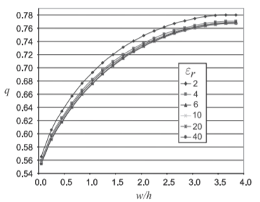
Figure \(\PageIndex{6}\): Dependence of the \(q\) factor of a microstrip line at \(1\text{ GHz}\) for various permittivities and aspect \((w/h)\) ratios. (Data obtained from EM field simulations using Sonnet.)
3.5.4 Filling Factor
Defining a filling factor, \(q\), provides useful insight into the distribution of energy in an inhomogeneous transmission line. The effective microstrip permittivity is\(^{2}\)
\[\label{eq:17}\varepsilon_{e}=1+q(\varepsilon_{r}-1) \]
where for a microstrip line \(q\) has the bounds
\[\label{eq:18}\frac{1}{2}\leq q\leq 1 \]
The useful aspect of \(q\) is that it is almost independent of \(\varepsilon_{r}\). A \(q\) factor of \(1\) would indicate that all of the fields are in the dielectric region. The dependence of the \(q\) of a microstrip line at \(1\text{ GHz}\) for various permittivities and aspect \((w/h)\) ratios is shown in Figure \(\PageIndex{6}\). The properties of a microstrip line, and uniform transmission lines in general, can be described very well by considering the geometric filling factor, \(q\), and the dielectric permittivity separately. Fitting of the microstrip data yields a formula for \(q\) in terms of the geometry parameters [19]:
\[\label{eq:19}q=\frac{1}{2}\left(1+\frac{1}{\sqrt{1+12h/w}}\right) \]
3.5.5 Microstrip Resistance
\(R\) for a microstrip line is the sum of the resistance of the strip and the resistance of the ground plane:
\[\label{eq:20}R=R_{\text{strip}}+R_{\text{ground}} \]
(with SI units of \(\Omega\text{/m}\)). At low frequencies the current is uniformly distributed in the strip and so
\[\label{eq:21}R_{\text{strip}}=\frac{\rho}{wt}=\frac{R_{s}}{w} \]
where \(\rho\) (with units of \(\Omega\text{m}\)) is the resistivity of the strip metal, \(R_{s} =\rho /t\) (with units of \(\Omega\) but referred to as \(\Omega\text{/sq}\), ohms per square) is the sheet resistance (also called the surface resistance) of the strip, \(t\) is the thickness of the strip, and \(w\) is the width of the strip. The sheet resistance is used to indicate the resistance of a sheet of conductor without needing to factor in the thickness \(t\) in calculations.
At DC the current is distributed in the ground plane over the full width of the ground. At quite low frequencies this transitions so that the current is not uniformly distributed in the ground plane and the resistance of the ground plane is approximated as [19]
\[\label{eq:22}R_{\text{ground}}=\frac{R_{sg}}{w}\frac{w/h}{w/h+5.8+0.03h/w},\quad\text{for }0.1\leq w/h\leq 10 \]
where the sheet resistance of the ground plane is \(R_{sg}\). The transition frequency from DC to the low-frequency approximation above has been found to be \(1.3\text{ MHz}\) for a microstrip with \(w = 200\:\mu\text{m}\), \(h = 100\:\mu\text{m}\), \(\varepsilon_{r} = 4\), and a ground plane width of \(2\text{ mm}\) (i.e., a very wide ground) [20]. So at RF and microwave frequencies Equation \(\eqref{eq:22}\) should be used as the low-frequency value of \(R_{\text{ground}}\). Both \(R_{\text{strip}}\) and \(R_{\text{ground}}\) will increase at higher frequencies as then the charges rearrange at much higher frequencies. This will be considered in the next chapter.
Finally, the attenuation due to the conductor loss, \(\alpha_{c}\), from Equation (2.5.15), is \(R/2Z_{0}\) and so
\[\label{eq:23}\alpha_{c}=\frac{R_{\text{strip}}+R_{\text{ground}}}{2Z_{0}} \]
If the strip in Example \(\PageIndex{2}\) has a resistance of \(1\:\Omega\text{/cm}\) and the ground plane resistance can be ignored, what is the attenuation constant at \(5\text{ GHz}\)?
Solution
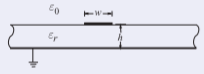
Figure \(\PageIndex{7}\)
For a low-loss line, \(\alpha = R/(2Z_{0})\) (since there is no dielectric loss), \(R =1\:\Omega\text{/cm},\: Z_{0} = 75.3\:\Omega\), and so, using Equation (2.5.15),
\[\alpha =0.664\text{ Np/m}\nonumber \]
3.5.6 Microstrip Conductance
For a microstrip line, an estimate of \(G\) is [19]
\[\label{eq:24}G=\frac{\varepsilon_{e}-1}{\varepsilon_{r}-1}\omega(\tan\delta)\varepsilon_{r}C_{\text{air}} \]
where \(\tan\delta\) is the loss tangent of the microstrip substrate and \(\omega\) is the radian frequency. So from Equations (2.5.14), \(\eqref{eq:4}\), and \(\eqref{eq:24}\),
\[\label{eq:25}\alpha_{d}=\frac{GZ_{0}}{2}=\frac{1}{2}\frac{\varepsilon_{e}-1}{\varepsilon_{r}-1}\omega(\tan\delta)\:\varepsilon_{r}C_{\text{air}}\frac{1}{c\sqrt{CC_{\text{air}}}} \]
Or, using Equation \(\eqref{eq:7}\), this can be written as
\[\label{eq:26}\alpha_{d}=\frac{\omega}{c}(\tan\delta)\frac{\varepsilon_{r}(\varepsilon_{e}-1)}{2\sqrt{\varepsilon_{e}}(\varepsilon_{r}-1)}\text{ Np/m} \]
This formula can be used with any TEM transmission line, that is, any transmission line in which the fields are perpendicular to the direction of propagation.
A rule of thumb is a guideline that is not intended to be accurate but can be easily applied. The accurate formulas for the characteristic impedance and effective permittivity of a microstrip line, Equations \(\eqref{eq:12}\)–\(\eqref{eq:16}\), indicate an underlying trend. The very approximate ‘rule of thumb,’ for characteristic impedance of a microstrip line is
\[\label{eq:27}Z_{0,\text{ ROT}}=\frac{k}{\sqrt{\varepsilon_{r}}}\sqrt{\frac{h}{w}} \]
where \(k\) is a constant which is established for a reference line. Taking the reference as \(\varepsilon_{r} = 10\) and \(w/h = 0.954\) then from Tables \(\PageIndex{1}\) and \(\PageIndex{2}\), \(Z_{0,\text{ REF}} = 50\:\Omega\). For this reference \(k = 154.4\:\Omega\). The following table indicates the accuracy of this rule of thumb.
| \(\varepsilon_{r}\) | \(w/h\) | actual \(Z_{0}\) (\(\Omega\)) | approzimate \(Z_{0,\text{ ROT}}\) (\(\Omega\)) | error |
|---|---|---|---|---|
| \(10\) | \(1\) | \(48.86\) | \(48.8\) | \(1\%\) |
| \(2\) | \(1\) | \(98.64\) | \(109\) | \(11\%\) |
| \(20\) | \(1\) | \(35.07\) | \(34.5\) | \(2\%\) |
| \(4\) | \(0.849\) | \(80\) | \(83.8\) | \(5\%\) |
| \(10\) | \(0.288\) | \(80\) | \(91.0\) | \(14\%\) |
| \(11.9\) | \(0.221\) | \(80\) | \(95.2\) | \(19\%\) |
| \(4\) | \(2.056\) | \(50\) | \(53.8\) | \(8\%\) |
| \(10\) | \(0.954\) | \(50\) | \(50.0\) | \(0\%\) |
| \(11.9\) | \(0.800\) | \(50\) | \(50.0\) | \(0\%\) |
| \(4\) | \(4.364\) | \(30\) | \(37.0\) | \(23\%\) |
| \(10\) | \(2.355\) | \(30\) | \(31.8\) | \(6\%\) |
| \(11.9\) | \(2.067\) | \(30\) | \(31.1\) | \(4\%\) |
Table \(\PageIndex{3}\)
Thus the trends are correctly described. Even the worst case (\(\varepsilon = 4,\: w/h = 4.364\)) has an error of \(23\%\) for a factor of \(11\) parameter change from the reference (\(\varepsilon = 10,\: w/h = 0.954\)).
Footnotes
[1] The assumption that \(L\) is not affected by the dielectric is a good approximation. However, there is a small discrepancy as a change in the electric field orientation affects the magnetic field, but there is little additional magnetic energy storage.
[2] The effective permittivity in Equation \(\eqref{eq:17}\) is the upper bound on the permittivity of mixtures [17] and is known as the Maxwell Garnett mixing rule [18].