
4.10: Lines on Semiconductor Substrates
- Page ID
- 41042

Propagation on transmission line structures fabricated on semiconductor substrates can have peculiar behavior. The interest in such lines is in relation to RF integrated circuits (RFICs) and monolithic microwave integrated circuits (MMICs) using both silicon and compound semiconductor technologies. More specifically, interconnects on metal-oxide-semiconductor (MOS) or metal-insulator-semiconductor (MIS) systems, where an insulating layer, such as oxide, exists between the conductor and the semiconductor wafer (see Figure \(\PageIndex{1}\)(a)), are of particular interest due to their ability to support a slow-wave mode. A slow-wave mode propagates much slower than would be expected. In the case of a semiconductor substrate with intermediate conductivity, the magnetic field penetrates into the substrate but the electric field does not. This separation of magnetic and electric fields slows the wave. Slow-wave structures find major use in distributed elements on-chip at RF. In particular, a silicon substrate can have a significant impact on microstrip propagation that derives from the charge layer formed at the silicon–silicon dioxide interface. The slow-wave effect is utilized in delay lines, couplers, and filters. With Schottky contact lines, the effect is used in variable-phase shifters, voltage-tunable filters, and various other applications.
Now, an intuitive explanation of the propagation characteristics of microstrip lines on layered substrates can be based on the parallel-plate structure shown in Figure \(\PageIndex{2}\). For an exact EM analysis of the slow-wave effect with silicon substrates, see [14]. As well as developing a very useful approximation for the important situation of transmission lines on an insulator such as silicon oxide on a semiconductor, the treatment below indicates the type of approach that can be used to analyze unusual structures. In this structure, assume a quasi-TEM mode of propagation. In other words, the wave propagation parameters \(\alpha,\:\beta,\) and \(Z_{0}\) can be deduced from electrostatic and magnetostatic solutions for the per unit length parameters \(C,\: G,\: L,\) and \(R\).
The analysis begins with a treatment of the classic Maxwell–Wagner capacitor. Figure \(\PageIndex{3}\)(a) shows the structure of such a capacitor where there are two different materials between the parallel plates of the capacitor with different permittivities and conductivities. The equivalent circuit is shown in
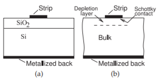
Figure \(\PageIndex{1}\): Transmission lines on silicon semiconductor: (a) silicon-silicon dioxide sandwich; and (b) bulk view.
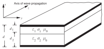
Figure \(\PageIndex{2}\): Parallel-plate transmission line structure.
Figure \(\PageIndex{3}\)(b) with the elements given by (\(A\) is the plate area)
\[\begin{align}\label{eq:1}C_{1}&=\varepsilon_{1}\frac{A}{d_{1}},\: R_{1}=\frac{1}{\sigma_{1}}\frac{d_{1}}{A},\:C_{2}=\varepsilon_{2}\frac{A}{d_{2}},\:R_{2}=\frac{1}{\sigma_{2}}\frac{d_{2}}{A} \\ \label{eq:2}\tau_{1}&=R_{1}C_{1}=\frac{\varepsilon_{1}}{\sigma_{1}},\:\tau_{2}=R_{2}C_{2}=\frac{\varepsilon_{2}}{\sigma_{2}}\end{align} \]
The admittance of the entire structure at radian frequency \(\omega\) is
\[\label{eq:3}Y(\omega)=\frac{1}{R_{1}+R_{2}}\frac{(1+\jmath\omega\tau_{1})(1+\jmath\omega\tau_{2})}{1+\jmath\omega\tau} \]
where
\[\label{eq:4}\tau=\frac{R_{1}\tau_{2}+R_{2}\tau_{1}}{R_{1}+R_{2}} \]
Introducing
\[\label{eq:5}Y(\omega)=\jmath\omega\left(\varepsilon_{e}\frac{A}{d}\right) \]
the effective complex permittivity, \(\varepsilon_{e} = \varepsilon_{e}' −\jmath\varepsilon_{e}''\), can be defined in terms of Equation \(\eqref{eq:3}\). Using Equations \(\eqref{eq:3}\) and \(\eqref{eq:5}\) yields
\[\label{eq:6}\varepsilon_{e}'=\frac{\tau_{1}+\tau_{2}-\tau+\tau\tau_{1}\tau_{2}\omega^{2}}{(R_{1}+R_{2})[1+(\omega\tau)^{2}]}\frac{d}{A} \]
Consider now the case when \(R_{1}\) goes to infinity (i.e., Layer \(\mathsf{1}\), the top layer, in Figure \(\PageIndex{3}\) is an insulator). For this case, Equation \(\eqref{eq:6}\) becomes
\[\label{eq:7}\varepsilon_{e}'=\frac{1+\left(1+\frac{d_{2}}{d_{1}}\frac{\varepsilon_{1}}{\varepsilon_{2}}\right)\left(\frac{\omega\varepsilon_{2}}{\sigma_{2}}\right)^{2}}{1+\left(1+\frac{d_{2}}{d_{1}}\frac{\varepsilon_{1}}{\varepsilon_{2}}\right)^{2}\left(\frac{\omega\varepsilon_{2}}{\sigma_{2}}\right)^{2}}\left(\varepsilon_{1}\frac{d}{d_{1}}\right) \]
It is clear from Equations \(\eqref{eq:6}\) and \(\eqref{eq:7}\) that the effective complex permittivity has a frequency-dependent component. Consider how this varies with a few cases of \(\omega\). For \(\omega = 0\), the static value of the effective permittivity is
\[\label{eq:8}\varepsilon_{e,0}'=\varepsilon_{1}\frac{d}{d_{1}} \]
For the case where \(\omega\) goes to infinity (the optical value), the real part of the effective permittivity is
\[\label{eq:9}\varepsilon_{e,\infty}'=\frac{\varepsilon_{1}\varepsilon_{2}(d_{1}+d_{2})}{\varepsilon_{2}d_{1}+\varepsilon_{1}d_{2}} \]
Note also that the value of \(\varepsilon_{e,\infty}′\) can be approximately achieved for a large value of \(\omega\varepsilon_{2}/\sigma_{2}\) (i.e., low-conductivity substrates can be used to ensure that the displacement currents dominate). In a similar way, it is clear that \(\varepsilon_{e,0}'\) can be achieved by having a small value of \(\omega\varepsilon_{2}/\sigma_{2}\). Also note that \(\varepsilon_{e,0}'\) can be made very large by making \(d_{1}\) much smaller than \(d\).
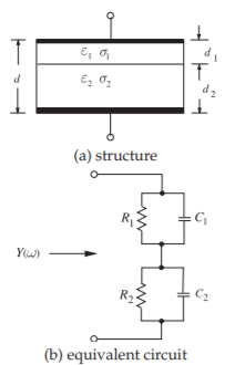
Figure \(\PageIndex{3}\): Maxwell–Wagner capacitor.
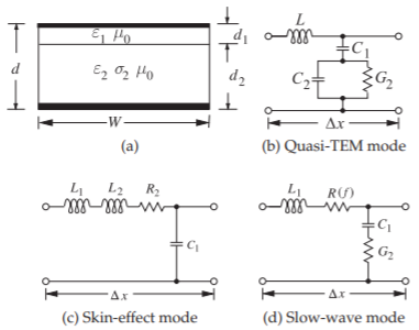
Figure \(\PageIndex{4}\): Modes on an MOS transmission line: (a) equivalent structure of the MOS line of Figure \(\PageIndex{1}\).
Consider the structure in Figure \(\PageIndex{2}\). Determine the guide wavelength, \(\lambda_{g}\), and the wavelength in the insulator, \(\lambda_{1}\), at a frequency of \(1\text{ GHz}\). SiO\(_{2}\) and Si are the dielectrics, with permittivities \(\varepsilon_{1} = 4\varepsilon_{0}\) and \(\varepsilon_{2} = 13\varepsilon_{0}\) (the conductivities are zero). The depths \(d_{2}\) and \(d_{1}\) of the two dielectrics are \(d_{2} = 250\:\mu\text{m}\) and \(d_{1} = 0.1\:\mu\text{m}\).
Solution
\[\begin{align}\lambda_{1}&=\frac{3\times10^{8}}{10^{9}\sqrt{4}}=0.15\text{ m}=15\text{ cm}\nonumber \\ \label{eq:10}\epsilon_{e}&=\frac{\varepsilon_{1}\varepsilon_{2}(d_{1}+d_{2})}{\varepsilon_{1}d_{2}+\varepsilon_{2}d_{1}}=12.99\varepsilon_{0},\quad\lambda_{g}=\frac{3\times10^{8}}{10^{9}\sqrt{12.99}}=0.0832\text{ m}=8.32\text{ cm}\end{align} \]
4.10.1 Modes on the MIS (MOS) Line
The previous description of the properties of a Maxwell–Wagner capacitor leads to a discussion of the possible modes on the MIS (MOS) line. To make the problem tractable, the transmission line shown in Figure \(\PageIndex{1}\)(a) will be approximated as having the cross section shown in Figure \(\PageIndex{4}\)(a).
Dielectric Quasi-TEM Mode
The first possible mode is the dielectric quasi-TEM mode, for which the sectional equivalent circuit model of Figure \(\PageIndex{4}\)(b) is applicable. In this mode \(\sigma_{2} ≪ \omega\varepsilon_{2}\). This implies from the earlier discussion that \(\varepsilon_{e}' = \varepsilon_{e,\infty}'\) and \(\mu_{e}' = \mu_{0}\). Thus the per unit length parameters are
\[\label{eq:11}L=\mu_{0}\frac{d_{1}}{W},\quad C_{1}=\varepsilon_{1}\frac{W}{d_{1}},\quad C_{2}=\varepsilon_{2}\frac{W}{d_{2}}m\quad G_{2}=\sigma_{2}\frac{W}{d_{2}} \]
These have the SI units \(\text{H/m}\) for \(L\), \(\text{F/m}\) for \(C_{1}\), \(\text{F/m}\) for \(C_{2}\), and \(\text{S/m}\) for \(G_{2}\).
Skin-Effect Mode
The second possible mode is the skin-effect mode, for which the sectional equivalent circuit model of Figure \(\PageIndex{4}\)(c) is applicable. Here, \(\sigma_{2} ≪ \omega\varepsilon_{2}\) is such that the skin depth \(\delta_{s} = 1/\sqrt{\pi f\mu_{0}\sigma_{2}}\) in the semiconductor is much smaller than \(d_{2}\) and
\[\varepsilon_{e}'=\varepsilon_{e,0}',\quad\mu_{e}'=\frac{\mu_{0}}{d}\left(d_{1}+\frac{\delta_{s}}{2}\right) \nonumber \]
Thus
\[\begin{align}\label{eq:12}L_{1}&=\mu_{0}\frac{d_{1}}{W},\quad&C_{1}&=\varepsilon_{1}\frac{W}{d_{1}}\\ \label{eq:13}L_{2}&=\mu_{0}\frac{1}{W}\left(\frac{\delta_{s}}{2}\right) &R_{2}&=2\pi f\mu_{0}\frac{1}{W}\left(\frac{\delta_{s}}{2}\right)\end{align} \]
These have the SI units \(\text{H/m}\) for \(L_{1}\) and \(L_{2}\), \(\text{F/m}\) for \(C_{1}\), and \(\Omega\text{/m}\) for \(R_{2}\).
Slow-Wave Mode
The third possible mode of propagation is the slow-wave mode [15, 16], for which the sectional equivalent circuit model of Figure \(\PageIndex{4}\)(d) is applicable. This mode occurs when \(f\) is not so large and the resistivity is moderate so that the skin depth, \(\delta_{s}\), is larger than (or on the order of) \(d_{2}\). Thus \(\varepsilon_{e}' =\varepsilon_{e,0}'\), but \(\mu_{e}' =\mu_{0}\). Therefore
\[\label{eq:14}v_{p}=\frac{1}{\sqrt{\varepsilon_{e}'\mu_{e}'}}=\frac{1}{\sqrt{\mu_{0}\varepsilon_{0}}}\frac{1}{\sqrt{\varepsilon_{1}}}\sqrt{\frac{d_{1}}{d}} \]
(with SI units of \(\text{m/s}\)) and \(\lambda_{g} =\lambda_{1}\sqrt{d_{1}/d}\), where \(\lambda_{1}\) is the wavelength in the insulator.