
5.8: Directional Coupler
- Page ID
- 41061

Coupling can be exploited to realize a new type of element called a directional coupler. The schematic of a directional coupler is shown in Figure \(\PageIndex{1}\)(a) and a microstrip realization is shown in Figure \(\PageIndex{1}\)(b). The microstrip realization is typical of most directional couplers in that it comprises two parallel signal lines with the electric and magnetic fields of a signal on one line inducing currents and voltages on the other. A usable directional
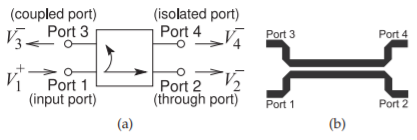
Figure \(\PageIndex{1}\): Directional couplers: (a) schematic; and (b) backward-coupled microstrip coupler. (Note that not all couplers are backward-wave couplers as shown in (a).)
| Parameter | Ideal | Ideal \((\text{dB})\) | Typical |
|---|---|---|---|
| Coupling, \(C\) | \(-\) | \(-\) | \(3-40\text{ dB}\) |
| Transmission, \(T\) | \(|\sqrt{1-1/C^{2}}|\) | \(20\log |\sqrt{1-1/C^{2}}|\) | \(-0.5\text{ dB}\) |
| Directivity, \(D\) | \(\infty\) | \(\infty\) | \(40\text{ dB}\) |
| Isolation, \(I\) | \(\infty\) | \(\infty\) | \(40\text{ dB}\) |
Table \(\PageIndex{1}\): Ideal and typical parameters of a directional coupler.
coupler has a coupled line length of at least one-quarter wavelength, with longer lengths of line resulting in broader bandwidth operation. Directional couplers are used to sample a traveling wave on one line and to induce a usually much smaller image of the wave on another line. That is, the forward- and backward-traveling waves are separated. Here a prescribed amount of the incident power is coupled out of the system. Thus, for example, a \(20\text{ dB}\) microstrip coupler is a pair of coupled microstrip lines in which \(1/100\) of the power input is coupled from one microstrip line onto the another.
Referring to Figure \(\PageIndex{1}\), a coupler is specified in terms of the following parameters (always check the magnitude of the factors, as some papers and books on couplers use the inverse of the \(C\) used here):
- Coupling factor:
\[\begin{aligned}C=V_{1}^{+}/V_{3}^{-}\quad =&\quad\text{inverse of the voltage fraction “transferred”} \\&\quad\text{(coupled) across to the opposite arm }(C>1)\end{aligned}\nonumber \] - Transmission factor (inverse of insertion loss):
\[\begin{aligned}T=V_{2}^{-}/V_{1}^{+}\quad =&\quad\text{transmission directly through the “primary” arm} \\&\quad\text{of the structure }(T<1)\end{aligned}\nonumber \] - Directivity factor:
\[\begin{aligned}D=V_{3}^{-}/V_{4}^{-}\quad =&\quad\text{measure of the undesired coupling from Port 1 to} \\&\quad\text{Port 4 relative to the signal level at Port 3 }(D>1)\end{aligned}\nonumber \] - Isolation factor:
\[\begin{aligned}I=V_{1}^{+}/V_{4}^{-}\quad =&\quad\text{isolation between Port 4 and Port 1 }(I>1)\end{aligned}\nonumber \]
It is usual to quote these quantities in decibels. For example, the coupling factor in decibels is \(C|_{\text{dB}} = 20 \log C\). So \(20\text{ dB}\) coupling indicates that the coupling factor is \(10\). An ideal quarter-wave coupler has \(D =\infty\) (i.e., infinite directivity) and
\[\label{eq:1}C=\frac{Z_{0e}+Z_{0o}}{Z_{0e}-Z_{0o}} \]
This result comes from a detailed derivation for the case when the coupled-line section is one-quarter wavelength long—the length when the coupling is maximum. The derivation is given in Section 11.4 of [5]. In decibels the coupling is
\[\label{eq:2}C|_{\text{dB}}=20\log\left(\frac{Z_{0e}+Z_{0o}}{Z_{0e}-Z_{0o}}\right) \]
Typical and ideal parameters of a directional coupler are given in Table \(\PageIndex{1}\). Since an ideal coupler does not dissipate power, the magnitude of the transmission coefficient is
\[\label{eq:3}|T|=|\sqrt{1-1/C^{2}}| \]
There are many types of directional couplers, and the phases of the traveling waves at the ports will not necessarily coincide. The microstrip coupler shown in Figure \(\PageIndex{1}\)(b) has maximum coupling when the lines are one-quarter wavelength long.\(^{1}\) At the frequency where they are one-quarter wavelength long, the phase difference between traveling waves entering at Port \(\mathsf{1}\) and leaving at Port \(\mathsf{2}\) will then be \(90^{\circ}\).
A lossless directional coupler has coupling \(C = 20\text{ dB}\), transmission factor \(0.8\), and directivity \(20\text{ dB}\). What is the isolation? Express your answer in decibels.
Solution
Coupling factor: \(C = V_{1}^{+}/V_{3}^{−}\)
Transmission factor: \(T = V_{2}^{−}/V_{1}^{+}\)
Directivity factor: \(D = V_{3}^{−}/V_{4}^{−}\)
Isolation factor: \(I = V_{1}^{+}/V_{4}^{−}\)
Figure \(\PageIndex{2}\)
\[D=20\text{ dB}=10\quad\text{and}\quad C=20\text{ dB}=10\nonumber \]
so the isolation is
\[I=\frac{V_{1}^{+}}{V_{4}^{-}}=\frac{V_{3}^{-}}{V_{4}^{-}}\cdot\frac{V_{1}^{+}}{V_{3}^{-}}=D\cdot C=10\cdot 10=100=40\text{ dB}\nonumber \]
5.8.1 Design Equations for a Directional Coupler
In the previous section the coupling factor was expressed in terms of the even- and odd-mode impedances. However, design starts with the specification of the coupling level, and from this the required physical dimensions are derived. A one-quarter wavelength long coupler will be considered, as this is the optimum coupling length. From Equation \(\eqref{eq:1}\), the desired coupling factor is
\[\label{eq:4}C=\frac{Z_{0e}+Z_{0o}}{Z_{0e}-Z_{0o}} \]
where the coupling factor is an absolute voltage-referenced quantity and usually must be derived from the coupling factor in decibels; let this be \(C|_{\text{dB}}\):
\[\label{eq:5}C=10^{C|_{\text{dB}}/20} \]
The system impedance comes from
\[\label{eq:6}Z_{0S}^{2}\approx Z_{0e}Z_{0o} \]
\(Z_{0S}\) is introduced here because \(Z_{0}\) is used for the characteristic impedance of the individual lines of the coupler; note that \(Z_{0}\) is not equal to \(Z_{0S}\). \(Z_{0S}\) should match the characteristic impedance of the transmission lines connected to the coupler. From these expressions, the even- and odd-mode impedances required are
\[\label{eq:7}Z_{0e}\approx Z_{0S}\sqrt{\frac{C+1}{C-1}} \]
\[\label{eq:8}Z_{0o}\approx Z_{0S}\sqrt{\frac{C-1}{C+1}} \]
and the ratio of imedances is
\[\label{eq:9}Z_{0e}/Z_{0o}\approx\frac{C+1}{C-1} \]
Develop the electrical design of a \(15\text{ dB}\) directional coupler in a \(50\:\Omega\) system.
Solution
The electrical design of a directional coupler comes down to determining the evenand odd-mode characteristic impedances required. Now the coupling factor, \(C\), is \((Z_{0e} + Z_{0o}) / (Z_{0e} − Z_{0o})\) and
\[Z_{0e}=Z_{0S}\sqrt{\frac{C+1}{C-1}}\nonumber \]
For a \(15\text{ dB}\) directional coupler, \(C = 15\text{ dB} = 5.618\) and, since \(Z_{0S} = 50\:\Omega\),
\[Z_{0e}=50\sqrt{\frac{5.618+1}{5.618-1}}=59.9\:\Omega\quad\text{and}\quad Z_{0o}=Z_{0S}^{2}/Z_{0e}=50^{2}/59.9=41.7\:\Omega\nonumber \]
The above are the required electrical design parameters.
5.8.2 Directional Coupler with Lumped Capacitors
Directional couplers using only coupled transmission lines can be large at low frequencies, as the minimum length is approximately one-quarter of a wavelength. This can be a problem at RF and low microwave frequencies, say, below \(3\text{ GHz}\). The length of the line can be reduced by incorporating lumped elements, as shown in Figure \(\PageIndex{3}\)(a). The equivalence is established using \(ABCD\) parameters. Figure \(\PageIndex{3}\)(b) shows a hybrid directional coupler using a ferrite core, forming a magnetic transformer, to provide enhanced coupling of the coupled lines at low frequencies with a frequency range of \(1–700\text{ MHz}\). At high frequencies the ferrite core is a magnetic open circuit and the line coupling dominates.
5.8.3 Physical Design of a Pair of Coupled Lines
Equations \(\eqref{eq:7}\)–\(\eqref{eq:9}\) are the basic design expressions, as \(Z_{0e}\) and \(Z_{0o}\) can be related to physical dimensions. When the two strips of a microstrip directional coupler are close, the orientation of the field lines and hence the characteristic impedances of the individual lines change. That is, the characteristic impedance of each line on its own, \(Z_{0}\), will differ from the system impedance, \(Z_{0S}\). For a normalized line width of \(u =(w/h)\), this effect is shown in Figure \(\PageIndex{4}\). Here \(Z_{0S}\) is the geometric mean of the even- and odd-mode impedances.
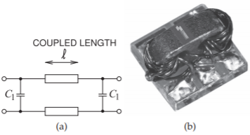
Figure \(\PageIndex{3}\): Parallel coupled lines with lumped capacitors bridging the ends to provide compensation: (a) schematic illustration; and (b) using a hybrid transformer to provide enhanced coupling of the coupled lines at low frequencies (Model GC6-2, copyright Synergy Microwave Corporation, used with permission [6]).
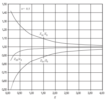
Figure \(\PageIndex{4}\): Normalized even- and odd-mode characteristic impedances of coupled microstrip lines with normalized width, \(u = 0.5\), versus normalized gap spacing, \(g\).
Microstrip coupler design proceeds as follows. The first step is to examine the specifications and determine the substrate permittivity, \(\varepsilon_{r}\), coupling factor, \(C\), and the system characteristic impedance, \(Z_{0S}\). From \(C\) find \(Z_{0e}/Z_{0}\); the data in Tables \(\PageIndex{2}\) and \(\PageIndex{3}\) enable some of the physical parameters to be determined, including the normalized gap coupling parameter, \(g\), and the normalized strip width, \(u\). The next step is to design the dimensions of the individual microstrip lines connecting the directional coupler using Table \(\PageIndex{3}\). At this stage the widths and spacings of the microstrip circuit are normalized. Using the substrate height, these are unnormalized to obtain the actual physical dimensions. Finally, the coupler is one-quarter wavelength long, as this was the basis for the formula relating the even- and odd-mode impedances to the coupling factor in Equation \(\eqref{eq:1}\). The even and odd modes have different effective permittivities and the \(\lambda_{g}/4\) length should apply to both the even and odd modes. Clearly both cannot be satisfied. It is reasonable to use the average of the even- and odd-mode permittivities to establish the coupler length. The length is not a very sensitive parameter anyway. The connection of the individual lines to the coupler is not specifically part of the synthesis described, but if designed they should have the system characteristic impedance.
A comment on this design procedure is in order. The design procedure above yields a narrowband directional coupler. A broadband directional coupler, and indeed any component that is desired to have a broad bandwidth, should be designed using filter principles. Another comment is that the design flow is one of synthesis. An alternative procedure that is often used is to start with an approximate design and rely on optimization tools to obtain the desired characteristics. This works in many cases, but does lead to novel design. Having said that, the synthesis procedure does not yield a perfect design, as parasitic and dispersive effects are not taken into account. Optimization from the synthesized design usually requires only a small adjustment. In practice, the uncertainties of physical structures (e.g., variations in the effective permittivity of actual materials) require experimental iteration as well.
| \(\varepsilon_{r}=4\) (SiO\(_{2}\) and FR4), \(Z_{0S}=50\:\Omega\) | |||||||
|---|---|---|---|---|---|---|---|
| \(g\) | \(Z_{0e}/Z_{0o}\) | \(u\) | \(Z_{0e}\) \((\Omega)\) | \(Z_{0o}\) \((\Omega)\) | \(\varepsilon_{ee}\) | \(\varepsilon_{eo}\) | \(Z_{0}\) \((\Omega)\) |
| \(0.1\) | \(2.20\) | \(1.57\) | \(74.12\) | \(33.72\) | \(3.20\) | \(2.61\) | \(58.60\) |
| \(0.2\) | \(1.87\) | \(1.72\) | \(68.38\) | \(36.52\) | \(3.23\) | \(2.65\) | \(55.60\) |
| \(0.3\) | \(1.70\) | \(1.80\) | \(65.26\) | \(38.37\) | \(3.25\) | \(2.68\) | \(54.10\) |
| \(0.4\) | \(1.59\) | \(1.86\) | \(62.93\) | \(39.66\) | \(3.26\) | \(2.70\) | \(53.10\) |
| \(0.5\) | \(1.50\) | \(1.90\) | \(61.26\) | \(40.74\) | \(3.27\) | \(2.72\) | \(52.20\) |
| \(0.6\) | \(1.44\) | \(1.93\) | \(59.93\) | \(41.63\) | \(3.27\) | \(2.74\) | \(52.00\) |
| \(0.7\) | \(1.39\) | \(1.95\) | \(58.90\) | \(42.42\) | \(3.27\) | \(2.76\) | \(51.60\) |
| \(0.8\) | \(1.35\) | \(1.97\) | \(57.95\) | \(43.05\) | \(3.28\) | \(2.78\) | \(51.30\) |
| \(0.9\) | \(1.31\) | \(1.98\) | \(57.25\) | \(43.67\) | \(3.28\) | \(2.79\) | \(51.20\) |
| \(1.0\) | \(1.28\) | \(1.99\) | \(56.61\) | \(44.20\) | \(3.27\) | \(2.80\) | \(51.00\) |
| \(1.2\) | \(1.23\) | \(2.01\) | \(55.46\) | \(45.03\) | \(3.27\) | \(2.82\) | \(50.70\) |
| \(1.4\) | \(1.19\) | \(2.02\) | \(54.64\) | \(45.76\) | \(3.27\) | \(2.84\) | \(50.50\) |
| \(1.6\) | \(1.16\) | \(2.03\) | \(53.93\) | \(46.32\) | \(3.26\) | \(2.85\) | \(50.40\) |
| \(1.8\) | \(1.14\) | \(2.03\) | \(53.48\) | \(46.88\) | \(3.25\) | \(2.87\) | \(50.40\) |
| \(2.0\) | \(1.12\) | \(2.04\) | \(52.94\) | \(47.21\) | \(3.25\) | \(2.88\) | \(50.20\) |
| \(2.5\) | \(1.09\) | \(2.05\) | \(52.08\) | \(47.91\) | \(3.23\) | \(2.91\) | \(50.10\) |
| \(3\) | \(1.07\) | \(2.05\) | \(51.62\) | \(48.46\) | \(3.20\) | \(2.93\) | \(50.10\) |
| \(4\) | \(1.04\) | \(2.06\) | \(50.93\) | \(48.98\) | \(3.17\) | \(2.96\) | \(49.90\) |
| \(5\) | \(1.03\) | \(2.06\) | \(50.64\) | \(49.35\) | \(3.15\) | \(2.98\) | \(49.90\) |
| \(10\) | \(1.00\) | \(2.07\) | \(50.06\) | \(49.89\) | \(3.10\) | \(3.02\) | \(49.80\) |
Table \(\PageIndex{2}\): Design parameters for coupled lines for \(\varepsilon_{r} = 4\). The normalized gap, \(g\), is chosen to obtain the desired coupled-line mode impedance ratio, \(Z_{0e}/Z_{0o}\). Data are derived from the analysis in Section 5.6. \(Z_{0}\) is the characteristic impedance of an individual microstrip line with a normalized width, \(u\). For \(Z_{0S} = 50\:\Omega,\: w/h = 2.056\), from Table 3.5.2.
| \(\varepsilon_{r}=10\) (Alumina), \(Z_{0S}=50\:\Omega\) | |||||||
|---|---|---|---|---|---|---|---|
| \(g\) | \(Z_{0e}/Z_{0o}\) | \(u\) | \(Z_{0e}\) \((\Omega)\) | \(Z_{0o}\) \((\Omega)\) | \(\varepsilon_{ee}\) | \(\varepsilon_{eo}\) | \(Z_{0}\) \((\Omega)\) |
| \(0.1\) | \(2.72\) | \(0.65\) | \(82.26\) | \(30.25\) | \(6.95\) | \(5.59\) | \(59.40\) |
| \(0.2\) | \(2.18\) | \(0.75\) | \(73.90\) | \(33.82\) | \(7.06\) | \(5.64\) | \(55.90\) |
| \(0.3\) | \(1.91\) | \(0.81\) | \(69.06\) | \(36.10\) | \(7.13\) | \(5.69\) | \(54.00\) |
| \(0.4\) | \(1.74\) | \(0.84\) | \(66.19\) | \(37.96\) | \(7.17\) | \(5.73\) | \(53.10\) |
| \(0.5\) | \(1.62\) | \(0.87\) | \(63.66\) | \(39.29\) | \(7.20\) | \(5.77\) | \(52.20\) |
| \(0.6\) | \(1.53\) | \(0.89\) | \(61.79\) | \(40.42\) | \(7.22\) | \(5.81\) | \(51.70\) |
| \(0.7\) | \(1.46\) | \(0.90\) | \(60.45\) | \(41.47\) | \(7.23\) | \(5.85\) | \(51.40\) |
| \(0.8\) | \(1.40\) | \(0.91\) | \(59.25\) | \(42.32\) | \(7.23\) | \(5.88\) | \(51.10\) |
| \(0.9\) | \(1.35\) | \(0.92\) | \(58.17\) | \(43.01\) | \(7.24\) | \(5.92\) | \(50.90\) |
| \(1.0\) | \(1.31\) | \(0.93\) | \(57.19\) | \(43.57\) | \(7.24\) | \(5.95\) | \(50.60\) |
| \(1.2\) | \(1.25\) | \(0.94\) | \(55.78\) | \(44.59\) | \(7.23\) | \(6.01\) | \(50.30\) |
| \(1.4\) | \(1.21\) | \(0.94\) | \(54.90\) | \(45.55\) | \(7.21\) | \(6.06\) | \(50.30\) |
| \(1.6\) | \(1.17\) | \(0.94\) | \(54.19\) | \(46.30\) | \(7.19\) | \(6.11\) | \(50.30\) |
| \(1.8\) | \(1.14\) | \(0.95\) | \(53.34\) | \(46.66\) | \(7.17\) | \(6.16\) | \(50.10\) |
| \(2.0\) | \(1.12\) | \(0.95\) | \(52.87\) | \(47.14\) | \(7.14\) | \(6.20\) | \(50.10\) |
| \(2.5\) | \(1.09\) | \(0.95\) | \(52.05\) | \(47.97\) | \(7.08\) | \(6.29\) | \(50.10\) |
| \(3\) | \(1.06\) | \(0.95\) | \(51.54\) | \(48.50\) | \(7.02\) | \(6.36\) | \(50.10\) |
| \(4\) | \(1.04\) | \(0.95\) | \(50.97\) | \(49.08\) | \(6.92\) | \(6.46\) | \(50.10\) |
| \(5\) | \(1.03\) | \(0.95\) | \(50.69\) | \(49.39\) | \(6.85\) | \(6.53\) | \(50.10\) |
| \(10\) | \(1.03\) | \(0.95\) | \(50.26\) | \(49.94\) | \(6.73\) | \(6.62\) | \(50.10\) |
Table \(\PageIndex{3}\): Design parameters for a microstrip coupler on a substrate with \(\varepsilon_{r}\) of \(10\). Data are derived from the analysis in Section 5.6. \(Z_{0}\) is the characteristic impedance of an individual microstrip line with a normalized width, \(u\). For \(Z_{0S} = 50\:\Omega,\: w/h = 0.954,\) from Table 3.5.2.
Design a microstrip directional coupler with the following specifications:
\[\begin{array}{lll}{\text{Transmission line technology}}&{\text{Microstrip}}&{}\\{\text{Coupling coefficient}}&{C}&{=10\text{ dB}}\\{\text{Microstrip characteristic impedance}}&{Z_{0}}&{=50\:\Omega}\\{\text{Substrate permittivity}}&{\varepsilon_{r}}&{=10.0}\\{\text{Substrate thickness}}&{h}&{=1\text{ mm}}\\{\text{System center frequency (midband for the coupler)}}&{f_{0}}&{=5\text{ GHz}}\end{array}\nonumber \]
The cross-sectional dimensions that must be determined are the strip width, \(w\), and the strip separation, \(s\), as shown in Figure \(\PageIndex{5}\). The procedure is to first determine the coupling factor:
\[\label{eq:10}C=10^{(C|_{\text{dB}}/20)}=10^{(10/20)}=3.162 \]
The ratio of the even- and odd-mode impedances required to achieve the desired coupling is derived from Equation \(\eqref{eq:9}\):
\[\label{eq:11}Z_{0e}/Z_{0o}=\frac{C+1}{C-1}=\frac{3.162+1}{3.162-1}=1.925 \]
Solution
The problem now is to determine the physical geometry (i.e., the line widths and spacing). The data in Table \(\PageIndex{3}\) apply here (as \(\varepsilon_{r} = 10\)), enabling the normalized gap, \(g = s/h\), and normalized line width, \(u = w/h\), to be determined for a specified impedance ratio, \(Z_{0e}/Z_{0o}\). The table does not contain a line for \(Z_{0e}/Z_{0o} = 1.925\) and so the table must be interpolated (e.g. using linear or bilinear interpolation as described in Appendix 1.A.12). The line for \(Z_{0e}/Z_{0o} = 2.15\) has \(g = 0.2\), and the line for \(Z_{0e}/Z_{0o} = 1.90\) has \(g = 0.3\). So for \(Z_{0e}/Z_{0o} = 1.925\),
\[\label{eq:12}g=\left(\frac{0.3-0.2}{1.9-2.15}\right)\cdot (1.925-2.15)+0.2=0.290 \]
thus
\[\label{eq:13}s=g\cdot h=0.290\text{ mm} \]
The value of \(u\) must also be interpolated from Table \(\PageIndex{3}\) and \(u = 0.805\) is obtained; thus
\[\label{eq:14}w=u\cdot h=0.805\text{ mm} \]
The coupler should be one-quarter wavelength long, so the effective relative permittivity of the even and odd modes is required. From Table \(\PageIndex{3}\), the interpolated values are
\[\label{eq:15}\varepsilon_{ee}=7.124\quad\text{and}\quad\varepsilon_{eo}=5.686 \]
These effective permittivities are different, so determination of the optimum length of the coupler is not straightforward. The only choice is to use the average of the permittivities:
\[\label{eq:16}\varepsilon_{e,\text{ avg}}=(\varepsilon_{ee}+\varepsilon_{eo})/2=6.405 \]
Thus the average wavelength is
\[\label{eq:17}\lambda_{g}=\frac{c}{f\sqrt{\varepsilon_{e,\text{ avg}}}}=\frac{3\cdot 10^{8}}{5\cdot 10^{9}\sqrt{6.405}}=2.37\text{ cm} \]
and the length of the coupler is
\[\label{eq:18}L=\lambda_{g}/4=5.93\text{ mm} \]
Finally, the widths of the feed lines must be determined. The system impedance is \(50\:\Omega\) and, from Table 3.5.2, the width, \(w′\), is found to be \(0.954\text{ mm}\). The final layout of the coupler is shown in Figure \(\PageIndex{6}\). The realization of a microstrip directional coupler as a laboratory component is shown in Figure \(\PageIndex{7}\).
EM analysis is often used to refine this synthesized coupler. There are two main uncertainties in the design. One is the uncertainty in the length of the coupler (due to the different even- and odd-mode effective permittivities). The other uncertainty is that the coupled-line equations come from low-frequency analysis—EM analysis will capture the frequency-dependent effects. However, only minor iteration would normally be required.
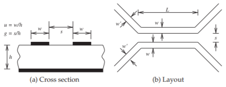
Figure \(\PageIndex{5}\): Dimensions to be determined in the physical design of a directional coupler.
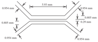
Figure \(\PageIndex{6}\): Final coupler layout for Example \(\PageIndex{3}\).
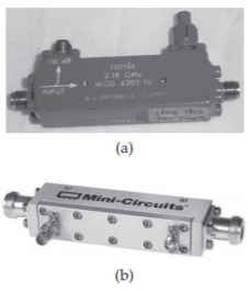
Figure \(\PageIndex{7}\): Connectorized directional couplers: (a) a microstrip directional coupler with SMA connectors connected to internal microstrip lines, the top right-hand connector has a \(50\:\Omega\) termination; (b) a \(250\text{ W},\: 0.9–9\text{ GHz}\) coupler with N-type connectors on the through line and an SMA connector on the coupled port, insertion loss is less than \(0.1\text{ dB}\). Copyright 2012 Scientific Components Corporation d/b/a Mini-Circuits, used with permission [7].
5.8.4 The Lange Coupler
A directional coupler comprised of two parallel microstrip lines cannot achieve a coupling of \(3\text{ dB}\), which corresponds to splitting the power of a traveling wave into two equal components. Lange [8] introduced a coupler, now known as the Lange coupler, in 1969. The Lange coupler (see Figure \(\PageIndex{8}\)) has a coupling factor of around \(3\text{ dB}\). In this design, true quadrature coupling over an octave bandwidth is realized as a consequence of the interdigital coupling section, which also compensates for the differences of the even- and odd-mode phase velocities over the wide frequency range. Note the use of the center bond wires—this was the key invention. The bonding wires should look, electrically, as close as possible to a short-
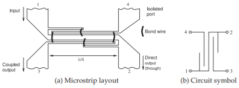
Figure \(\PageIndex{8}\): A four-finger Lange coupler.
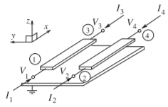
Figure \(\PageIndex{9}\): Coupled microstrip lines with total voltage and current phasors at the four terminals.
circuit. This means that their lengths, \(l_{s}\), must be kept as short as possible: ls \(≪ \lambda_{gm}/4\), where \(\lambda_{gm}\) is the midband wavelength. In semiconductor technologies, these bond wires are replaced by air bridges, and in structures with two or more metal layers the wirebonds are replaced by vias to another metal layer and a short connection on the second metal layer. In some designs, six coupling fingers are used instead of the four shown in Figure \(\PageIndex{8}\). Note that the input-to-direct-output link meanders through the structure and this DC connection identifies the through connection.
The physical length of the coupler is approximately one-quarter wavelength long at the center frequency of the coupling band. As with many distributed components, this element was invented using intuition and empirical iterations. Since then, analytic design formulas have been developed to enable synthesis of the electrical parameters of the coupler (see [5]). The synthesis is based on even- and odd-mode impedances analogous to those developed in Section 5.8 for a coupler comprised of coupled microstrip lines. Synthesis leads to a design that is close to ideal, and subsequent modeling in an EM simulator can be used to obtain an optimized design accounting for frequency-dependent and parasitic effects.
Footnotes
[1] This is shown in a detailed derivation provided in Section 11.4 of [5].