
5.9: Models of Parallel Coupled Lines
- Page ID
- 41062

5.9.1 Chain Matrix Model of Coupled Lines
The chain matrix of a pair of coupled lines is the multiport version of the two-port \(ABCD\) parameters and relates the input currents and voltages at one end of a pair of coupled lines to the voltages and currents at the other end. The chain matrix is derived here following the development in [9]. The terminal characteristics of the coupled lines shown in Figure 5.8.9 can be expressed in terms of the even and odd modes. For the even mode
\[\label{eq:1}\left[\begin{array}{c}{\frac{1}{2}(V_{1}+V_{2})}\\{\frac{1}{2}(I_{1}+I_{2})}\end{array}\right] =\left[\begin{array}{cc}{\cos\theta_{e}}&{\jmath X_{0e}\sin\theta_{e}}\\{\jmath Y_{0e}\sin\theta_{e}}&{\cos\theta_{e}}\end{array}\right]\left[\begin{array}{c}{\frac{1}{2}(V_{3}+V_{4})}\\{\frac{1}{2}(I_{3}+I_{4})}\end{array}\right] \]
and for the odd mode
\[\label{eq:2}\left[\begin{array}{c}{\frac{1}{2}(V_{1}-V_{2})}\\{\frac{1}{2}(I_{1}-I_{2})}\end{array}\right] =\left[\begin{array}{cc}{\cos\theta_{o}}&{\jmath X_{0o}\sin\theta_{o}}\\{\jmath Y_{0o}\sin\theta_{o}}&{\cos\theta_{o}}\end{array}\right]\left[\begin{array}{c}{\frac{1}{2}(V_{3}-V_{4})}\\{-\frac{1}{2}(I_{3}-I_{4})}\end{array}\right] \]
where \(Y_{0e} = 1/Z_{0e}\) is the even-mode characteristic admittance and \(Y_{0o} = 1/Z_{0o}\) is the characteristic admittance of the odd mode. Also, \(\theta_{e}\) is the electrical length of the lines for the even mode, and \(\theta_{o}\) is the odd-mode electrical length of the lines. Grouping Equations \(\eqref{eq:1}\) and \(\eqref{eq:2}\),
\[\label{eq:3}\left[\begin{array}{c}{V_{1}}\\{V_{2}}\\{I_{1}}\\{I_{2}}\end{array}\right] =\left[\begin{array}{cccc}{a_{11}}&{a_{12}}&{b_{11}}&{b_{12}}\\{a_{21}}&{a_{22}}&{b_{21}}&{b_{22}}\\{c_{11}}&{c_{12}}&{d_{11}}&{d_{12}}\\{c_{21}}&{c_{22}}&{d_{21}}&{d_{22}}\end{array}\right]\left[\begin{array}{c}{V_{3}}\\{V_{4}}\\{-I_{3}}\\{-I_{4}}\end{array}\right] \]
where
\[\begin{align}\label{eq:4}a_{11}&=a_{22}=d_{11}=d_{11}=\frac{1}{2}(\cos\theta_{e}+\cos\theta_{o}) \\ \label{eq:5}a_{12}&=a_{21}=d_{12}=d_{21}=\frac{1}{2}(\cos\theta_{e}-\cos\theta_{o}) \\ \label{eq:6}b_{11}&=b_{22}=\jmath\frac{1}{2}(Z_{0e}\sin\theta_{e}+Z_{0o}\sin\theta_{o}) \\ \label{eq:7}b_{12}&=b_{21}=\jmath\frac{1}{2}(Z_{0e}\sin\theta_{e}-Z_{0o}\sin\theta_{o}) \\ \label{eq:8}c_{11}&=c_{22}=\jmath\frac{1}{2}(Y_{0e}\sin\theta_{e}+Y_{0o}\sin\theta_{o}) \\ \label{eq:9}c_{12}&=c_{21}=\jmath\frac{1}{2}(Y_{0e}\sin\theta_{e}-Y_{0o}\sin\theta_{0})\end{align} \]
Similarly the admittance equation for a pair of coupled lines is derived as
\[\label{eq:10}\left[\begin{array}{c}{V_{1}}\\{V_{2}}\\{V_{3}}\\{V_{4}}\end{array}\right] =\left[\begin{array}{cccc}{y_{11}}&{y_{12}}&{y_{13}}&{y_{14}} \\ {y_{21}}&{y_{22}}&{y_{23}}&{y_{24}} \\ {y_{31}}&{y_{32}}&{y_{33}}&{y_{34}} \\ {y_{41}}&{y_{42}}&{y_{43}}&{y_{44}}\end{array}\right]\left[\begin{array}{c}{I_{1}}\\{I_{2}}\\{I_{3}}\\{I_{4}}\end{array}\right] \]
where
\[\begin{align} \label{eq:11} y_{11}&=y_{22}=y_{33}=y_{44}=-\jmath\frac{1}{2}(Y_{0e}\cot\theta_{e}+Y_{0o}\cot\theta_{o}) \\ \label{eq:12} y_{12}&=y_{21}=y_{34}=y_{43}=-\jmath\frac{1}{2}(Y_{0e}\cot\theta_{e}-Y_{0o}\cot\theta_{o}) \\ \label{eq:13} y_{13}&=y_{31}=y_{24}=y_{42}=\jmath\frac{1}{2}(Y_{0e}\csc\theta_{e}+Y_{0o}\csc\theta_{o}) \\ \label{eq:14} y_{14}&=y_{41}=y_{23}=y_{32}=\jmath\frac{1}{2}(Y_{0e}\csc\theta_{e}-Y_{0o}\csc\theta_{o})\end{align} \]
5.9.2 \(ABCD\) Parameters of Coupled-Line Sections
The chain matrix of a pair of coupled lines, Equation \(\eqref{eq:3}\), can be used to develop the \(ABCD\) parameters of two-port coupled line networks [9]. Several networks that are commonly used in realizing filters and other microwave circuits are shown in Table \(\PageIndex{1}\) with
\[\label{eq:15}\left[\begin{array}{c}{V_{1}}\\{I_{1}}\end{array}\right]=\left[\begin{array}{cc}{A}&{B}\\{C}&{D}\end{array}\right]\left[\begin{array}{c}{V_{2}}\\{-I_{2}}\end{array}\right] \]
One approach to developing the physical layout of microwave circuits from the electrical design equates the \(ABCD\) parameters of the coupled-line networks to the \(ABCD\) of the synthesized lumped-element circuit.
5.9.3 Synthesis of Specific Coupled-Line Connections
The equivalence of \(ABCD\) parameters can be used in microwave network synthesis to transform uncoupled transmission line structures into a
(a) Open-circuited interdigital coupled-line section (bandpass/bandstop networks)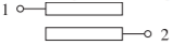 \[\begin{align}A&=D=(Z_{0e}\cot\theta_{e}+Z_{0o}\cot\theta_{o})/\Delta\nonumber \\ B&=\frac{\jmath}{2\Delta}[Z_{0e}^{2}+Z_{0o}^{2} \nonumber \\ &\quad −2Z_{0e}Z_{0o} (\cot\theta_{e}\cot\theta_{o} + \csc\theta_{e}\csc\theta_{o})]\nonumber \\ C&=2\jmath/\Delta\nonumber \\ \label{eq:16}\Delta&=Z_{0e}\csc\theta_{e} − Z_{0o}\csc\theta_{o}\end{align} \] |
(b) Short-circuited interdigital coupled-line section (bandpass/bandstop networks)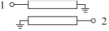 \[\begin{align}A&=D=(Y_{0e}\cot\theta_{e}+ Y_{0o}\cot\theta_{o})/\Delta\nonumber \\ B&=2\jmath/\Delta\nonumber \\ C&=\frac{\jmath}{2\Delta}[Y_{0e}^{2}+Y_{0o}^{2}\nonumber \\ &\quad −2Y_{0e}Y_{0o} (\cot\theta_{e}\cot\theta_{o} + \csc\theta_{e}\csc\theta_{o})]\nonumber \\ \label{eq:17}\Delta&= Y_{0e}\csc\theta_{e} − Y_{0o}\csc\theta_{o}\end{align} \] |
(c) Meander coupled-line section (lowpass networks)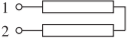 \[\begin{align}A&=D= (Z_{0e}\cot\theta_{e} − Z_{0o}\cot\theta_{o})/\Delta\nonumber \\ B&=2\jmath 2Z_{0e}Z_{0o} \cot\theta_{e}\tan\theta_{o}/\Delta\nonumber \\ C&=2\jmath/\Delta\nonumber \\ \label{eq:18}\Delta&=Z_{0e}\cot\theta_{e}+Z_{0o}\tan\theta_{o}\end{align} \] |
(d) Shorted symmetric coupled-line section (lowpass networks)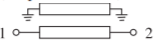 \[\begin{align}A&=D=(Y_{0e}\cot\theta_{e} + Y_{0o}\cot\theta_{o})/\Delta\nonumber \\ B&=2\jmath/\Delta\nonumber \\ C&=[\jmath /(2\Delta)] [Y_{0e}^{2} + Y_{0o}^{2}\nonumber \\ &\quad +2Y_{0e}Y_{0o} (\csc\theta_{e}\csc\theta_{o}− \cot\theta_{e}\cot\theta_{o})]\nonumber \\ \label{eq:19}\Delta &=Y_{0e}\csc\theta_{e} + Y_{0o}\csc\theta_{o}\end{align} \] |
(e) Open-circuited combine coupled-line section (bandpass/bandstop networks) \[\begin{align}A&=D= (Z_{0e}\cot\theta_{e}+ Z_{0o}\cot\theta_{o})/\Delta\nonumber \\ B &= −\jmath 2Z_{0e}Z_{0o}\cot\theta_{e}\cot\theta_{o}/\Delta\nonumber \\ C&=2\jmath/\Delta\nonumber \\ \label{eq:20}\Delta&=Z_{0e}\cot\theta_{e} − Z_{0o}\cot\theta_{o}\end{align} \] |
(f) Short-circuited combine coupled-line section (bandpass/bandstop networks) \[\begin{align}A&=D = (Y_{0o}\cot\theta_{o} + Y_{0e}\cot\theta_{e})/\Delta\nonumber \\ B&=2\jmath/\Delta\nonumber \\ C&= −\jmath 2Y_{0e}Y_{0o}\cot\theta_{e}\cot\theta_{o}/\Delta\nonumber \\ \label{eq:21}\Delta&=Y_{0o}\cot\theta_{o} − Y_{0e}\cot\theta_{e}\end{align} \] |
Table \(\PageIndex{1}\): \(ABCD\) parameters of coupled-line sections. Usage described in [10, 11, 12, 13].
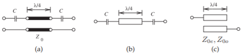
Figure \(\PageIndex{1}\): Coupled line equivalence: (a) a one-quarter wavelength long line with input and output series capacitance; (b) microstrip layout; and (c) equivalent coupled lines laid out in microstrip. The network in (a) is equivalent to the network in (c) if \(Z_{0e} = (1/C + 2Z_{0})\) and \(Z_{0o} = Z_{0}\).
coupled-line section. As an example, consider the capacitively coupled one-quarter wavelength long line shown in both Figures \(\PageIndex{1}\)(a) and \(\PageIndex{1}\)(b). This configuration often occurs in filter design and an equivalent structure using coupled lines and not requiring discrete capacitors is shown in Figure \(\PageIndex{1}\)(c). The equivalence is developed by equating the \(ABCD\) parameters of the two
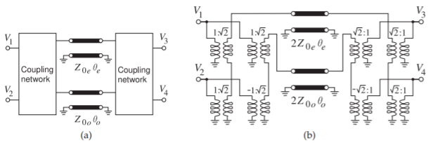
Figure \(\PageIndex{2}\): Models of a pair of coupled lines using even- and odd-mode lines: (a) with coupling network; and (b) with transformer-based coupling.
structures. The \(ABCD\) matrix of the coupled-line network of Figure \(\PageIndex{1}\)(c) is given in Table \(\PageIndex{1}\)(a):
\[\begin{align} A&=\frac{Z_{0e}\cot\theta_{e} + Z_{0o}\cot\theta_{o}}{Z_{0e}\csc\theta_{e} − Z_{0o}\csc\theta_{o}}=D &C&=\frac{2\jmath}{Z_{0e}\csc\theta_{e} − Z_{0o}\csc\theta_{o}}\nonumber \\ \label{eq:22}B&=\frac{\jmath}{2}\frac{Z_{0e}^{2} + Z_{0o}^{2} − 2Z_{0e}Z_{0o} (\cot\theta_{e}\cot\theta_{o} + \csc\theta_{e}\csc\theta_{o})}{Z_{0e}\csc\theta_{e} − Z_{0o}\csc\theta_{o}}\end{align} \]
where \(Z_{0e}\) and \(Z_{0o}\) are the modal impedances, and \(\theta_{e}\) and \(\theta_{o}\) are the even-and odd-mode electrical lengths.
Developing the \(ABCD\) parameters of the capacitively loaded one-quarter wavelength long line in Figure \(\PageIndex{1}\)(a) and equating them with the \(ABCD\) parameters in Equation \(\eqref{eq:22}\) leads to an equivalence between the loaded line (Figure \(\PageIndex{1}\)(b)) and the coupled line shown in Figure \(\PageIndex{1}\)(c), where
\[\label{eq:23}Z_{0e}= (1/C + 2Z_{0})\quad\text{and}\quad Z_{0o} = Z_{0} \]
5.9.4 Model Using Even- and Odd-Mode Lines
The pair of coupled lines in Figure 5.8.9 can be modeled using evenand odd- mode transmission lines as shown in Figure \(\PageIndex{2}\)(a). While the partitioning of the terminal voltages and currents of the coupled lines into even- and odd-mode components is simple to describe mathematically (e.g., the odd-mode voltage \(V_{o} =\frac{1}{2}(V_{1} − V_{2})\)), there is not a simple way to represent the partitioning in circuit form. Instead, in a circuit simulator the coupling network in Figure \(\PageIndex{2}\)(a) is modeled using voltage-controlled current sources [14]. A circuit model that is more convenient to use in the analysis of a coupled line networks is shown in Figure \(\PageIndex{2}\)(b). The equivalence of this network to a coupled line is demonstrated by showing that the chain matrix parameters of the circuit in Figure \(\PageIndex{2}\)(b) are the same as those in Equations \(\eqref{eq:3}\)–\(\eqref{eq:9}\), see Example \(\PageIndex{1}\).
Coupled lines are an important element in many microwave circuits, including filters, matching networks, and biasing networks. Very often the circuit development leads to a particular topology that can be implemented using coupled-line networks. For example, the structure at the top in Figure \(\PageIndex{3}\)(a) is known as an open-circuited interdigital section. The equivalent
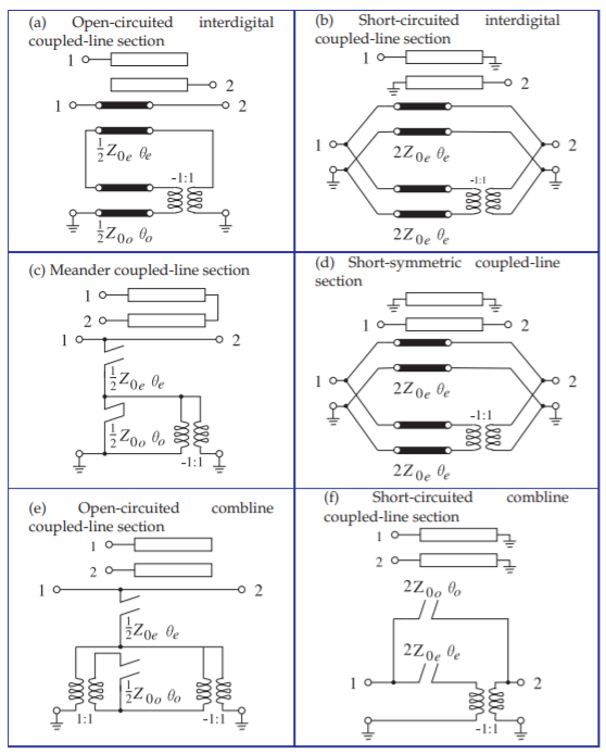
Figure \(\PageIndex{3}\): Coupled-line sections with models comprising individual transmission lines corresponding to the even- and odd-modes.
circuit of this network, shown at the bottom in Figure \(\PageIndex{3}\)(a), is derived from the coupled-line equivalent circuit shown in Figure \(\PageIndex{2}\)(b).
Develop the chain matrix of the coupled-line model shown in Figure \(\PageIndex{2}\)(b) and show that these are the chain matrix parameters of a coupled line.
Solution
The coupled-line model is annotated with voltages and currents in Figure \(\PageIndex{4}\). Using Table 2.A.1 of [15], the even- and odd-mode lines have the following \(ABCD\) parameters:
\[\begin{align}\label{eq:24}\left[\begin{array}{c}{V_{W}}\\{I_{W}}\end{array}\right]&=\left[\begin{array}{cc}{\cos\theta_{e}}&{\jmath 2Z_{e}\sin\theta_{e}}\\{\jmath\frac{1}{e}Y_{e}\sin\theta_{e}}&{\cos\theta_{e}}\end{array}\right]\left[\begin{array}{c}{V_{Y}}\\{I_{Y}}\end{array}\right] \\ \label{eq:25}\text{and}\quad\left[\begin{array}{c}{V_{X}}\\{I_{X}}\end{array}\right]&=\left[\begin{array}{cc}{\cos\theta_{o}}&{\jmath 2Z_{o}\sin\theta_{o}}\\{\jmath\frac{1}{2}Y_{o}\sin\theta_{o}}&{\cos\theta_{o}}\end{array}\right]\left[\begin{array}{c}{V_{Z}}\\{I_{Z}}\end{array}\right]\end{align} \]
While the \(ABCD\) parameters of the transformers could be used, it is more convenient to write down the terminal characteristics of the transformers directly. First, the transformers on the right-hand side are described by
\[\begin{array}{cc}{V_{Y} = \frac{1}{\sqrt{2}}(V_{3} + V_{4})}&{I_{Y}=\frac{1}{2\sqrt{2}}[(-I_{3})+(-I_{4})]}\\ \label{eq:26}{}&{} \\ {V_{Z}=\frac{1}{\sqrt{2}}(V_{3}-V_{4})}&{I_{Z}=\frac{1}{2\sqrt{2}}[(-I_{3})-(-I_{4})]}\end{array} \]
Combining Equations \(\eqref{eq:24}\)–\(\eqref{eq:26}\) yields
\[\label{eq:27}\left[\begin{array}{c}{V_{W}}\\{V_{X}}\\{I_{W}}\\{I_{X}}\end{array}\right]=\left[\begin{array}{cccc}{\sqrt{2}\cos\theta_{e}}&{\sqrt{2}\cos\theta_{e}}&{\jmath\sqrt{2}Z_{0e}\sin\theta_{e}}&{\jmath\sqrt{2}Z_{0e}\sin\theta_{e}}\\{\sqrt{2}\cos\theta_{o}}&{-\sqrt{2}\cos\theta_{o}}&{\jmath\sqrt{2}Z_{0o}\sin\theta_{o}}&{-\jmath\sqrt{2}Z_{0o}\sin\theta_{o}}\\{\jmath\frac{1}{2\sqrt{2}}Y_{0e}\sin\theta_{e}}&{\jmath\frac{1}{2\sqrt{2}}Y_{0e}\sin\theta_{e}}&{\frac{1}{2\sqrt{2}}\cos\theta_{e}}&{\frac{1}{2\sqrt{2}}\cos\theta_{e}}\\{\jmath\frac{1}{2\sqrt{2}}Y_{0o}\sin\theta_{o}}&{-\jmath\frac{1}{2\sqrt{2}}Y_{0o}\sin\theta_{o}}&{\frac{1}{2\sqrt{2}}\cos\theta_{o}}&{-\frac{1}{2\sqrt{2}}\cos\theta_{o}} \end{array}\right]\left[\begin{array}{c}{V_{3}}\\{V_{4}}\\{-I_{3}}\\{-I_{4}}\end{array}\right] \]
The development is completed by using the voltage and current relations determined by the transformers on the left-hand side:
\[\begin{array}{cc}{V_{1}=\frac{1}{2\sqrt{2}}(V_{W}+V_{X})}&{I_{1}=\sqrt{2}(I_{W}+I_{X})}\\ \label{eq:28}{}&{}\\{V_{2}=\frac{1}{2\sqrt{2}}(V_{W}-V_{X})}&{I_{2}=\sqrt{2}(I_{W}-I_{X})}\end{array} \]
Combining Equations \(\eqref{eq:27}\) and \(\eqref{eq:28}\):
\[\label{eq:29}\left[\begin{array}{c}{V_{1}}\\{V_{2}}\\{I_{1}}\\{I_{2}}\end{array}\right]=\left[\begin{array}{cccc}{a_{11}'}&{a_{12}'}&{b_{11}'}&{b_{12}'}\\{a_{21}'}&{a_{22}'}&{b_{21}'}&{b_{22}'}\\{c_{11}'}&{c_{12}'}&{d_{11}'}&{d_{12}'}\\{c_{21}'}&{c_{22}'}&{d_{21}'}&{d_{22}'}\end{array}\right]\left[\begin{array}{c}{V_{3}}\\{V_{4}}\\{-I_{3}}\\{-I_{4}}\end{array}\right] \]
where
\[\begin{aligned} a_{11}'&= a_{22}'= d_{11}' = d_{22}' = \frac{1}{2}(\cos\theta_{e} + \cos\theta_{o}) &a_{12}'&= a_{21}' = d_{12}' = d_{21}' =\frac{1}{2}(\cos\theta_{e} − \cos\theta_{o}) \\ b_{11}'&= b_{22}' =\jmath\frac{1}{2} (Z_{0e} \sin\theta_{e} + Z_{0o} \sin\theta_{o}) &b_{12}'&= b_{21}' = \jmath\frac{1}{2}(Z_{0e} \sin\theta_{e} − Z_{0o}\sin\theta_{o}) \\ c_{11}'&= c_{22}' = \jmath\frac{1}{2} (Y_{0e} \sin\theta_{e} + Y_{0o}\sin\theta_{c}) &c_{12}'&= c_{21}' =\jmath\frac{1}{2} (Y_{0e} \sin\theta_{e} − Y_{0o} \sin\theta_{o})\end{aligned}\nonumber \]
which is identical to the chain matrix of the coupled transmission line, Equation \(\eqref{eq:3}\). Thus Figure \(\PageIndex{2}\)(b) is an accurate circuit model of a pair of coupled transmission lines.
5.9.5 Alternative Coupled-Line Model
The previous section developed a model of a pair of coupled lines and it was shown how the model related to various coupled-line sections. While \(ABCD\) parameters can be used to equate two different implementations, it is useful to have a topology that can be visualized and used to guide synthesis.
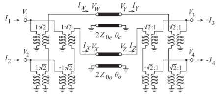
Figure \(\PageIndex{4}\): Annotated coupled-line model used in Example 5.7.2.
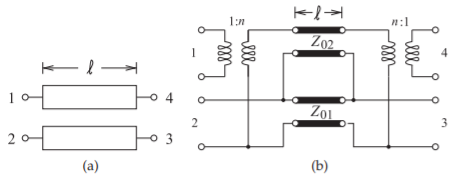
Figure \(\PageIndex{5}\): A pair of symmetrical coupled lines: (a) physical layout; and (b) its approximate equivalent circuit model in a form that appears in network synthesis. \(n = (Z_{0e} + Z_{0o})/(Z_{0e} − Z_{0o})\).
The accurate form of the coupled-line model developed in the previous section does not often occur in network synthesis. (In synthesis, such as when designing a filter using coupled lines, a mathematical description can sometimes be converted into circuit form which includes transmission lines that are coupled.) An alternative but approximate model that has the same topology as many synthesized networks is shown in Figure \(\PageIndex{5}\)(b).
A physical pair of coupled lines is shown in Figure \(\PageIndex{5}\)(a) with even-mode characteristic impedance, \(Z_{0e}\), and odd-mode impedance, \(Z_{0o}\), with the coupling coefficient\(^{1}\)
\[\label{eq:30} K=\frac{Z_{0e}-Z_{0o}}{Z_{0e}+Z_{0o}} \]
The corresponding approximate equivalent network model of the coupled line in Figure \(\PageIndex{5}\)(a) was developed by Malherbe [16] and is shown in Figure \(\PageIndex{5}\)(b) with
\[\begin{align}\label{eq:31} Z_{01}&=\frac{Z_{0S}}{\sqrt{1-K^{2}}} \\ \label{eq:32} Z_{02}&=Z_{0S}\frac{\sqrt{1-K^{2}}}{K^{2}} \\ \label{eq:33}n&=\frac{1}{K}=\frac{Z_{0e}+Z_{0o}}{Z_{0e}-Z_{0o}} \\ \label{eq:34}Z_{0S}&=\sqrt{Z_{0e}Z_{0o}}\end{align} \]
The electrical length of the \(Z_{01}\) and \(Z_{02}\) lines is the electrical length of the coupled line. The reason this model is approximate is it assumes that the coupled lines are symmetrical (e.g., equal width for the microstrip lines) and uses a low-frequency capacitor-based development. Also a pair of coupled lines has two electrical lengths, the electrical length of the even mode and the electrical length of the odd mode. So the best that can be done is to take the electrical lengths of the \(Z_{01}\) and \(Z_{02}\) lines as the average electrical lengths of the even and odd modes. Never-the-less this model is commonly used in developing the initial design of coupled-line networks that must then be followed by adjustment in a microwave circuit simulator.
5.9.6 Approximate Synthesis from the Coupled-Line Model
The electrical design of networks of coupled lines commonly leads to the parameters of the coupled-line model shown in Figure \(\PageIndex{5}\)(b). From these the physical layout can be derived. That is, given \(n = 1/K,\: Z_{01},\) and \(Z_{02}\), the coupled-line parameters \(Z_{0S},\: Z_{0e},\) and \(Z_{0o}\) are found. Equations \(\eqref{eq:31}\) and \(\eqref{eq:32}\) lead to two equations for \(Z_{0S}\):
\[\begin{align}\label{eq:35}Z_{0S, (5.197)}&=Z_{01}\sqrt{1-K^{2}} \\ \label{eq:36}Z_{0S, (5.198)}&=Z_{02}\frac{K^{2}}{\sqrt{1-K^{2}}}\end{align} \]
These could be different and this is a result of the model being approximate. If so, then the proper course forward is to use the geometric mean:
\[\label{eq:37}Z_{0S}=\sqrt{Z_{0S, (5.197)}Z_{0S, (5.198)}} \]
Rearranging Equation \(\eqref{eq:33}\),
\[\begin{align}1+n&=1+\frac{Z_{0e}+Z_{0o}}{Z_{0e}-Z_{0o}}=\frac{Z_{0e}-Z_{0o}+Z_{0e}+Z_{0o}}{Z_{0e}-Z_{0o}}=\frac{2Z_{0e}}{Z_{0e}-Z_{0o}} \nonumber \\ \label{eq:38} 1-\frac{2}{n+1}&=\frac{n-1}{n+1}=1-\frac{Z_{0e}-Z_{0o}}{Z_{0e}}=\frac{Z_{0o}-Z_{0e}+Z_{0e}}{Z_{0e}}=\frac{Z_{0o}}{Z_{0e}}\end{align} \]
That is,
\[\label{eq:39}\frac{Z_{0e}}{Z_{0o}}=\frac{n+1}{n-1} \]
Combining this with Equation \(\eqref{eq:34}\),
\[\label{eq:40}Z_{0o}=Z_{0S}\sqrt{\frac{n-1}{n+1}}\quad\text{and}\quad Z_{0e}=\frac{Z_{0S}^{2}}{Z_{0o}} \]
These equations can be used in physical synthesis. For example, if \(Z_{0S}\) is close to \(50\:\Omega\) and the substrate is alumina, then the ratio \(Z_{0e}/Z_{0o}\) can be used to find the physical dimensions from Table 5.8.3. Otherwise the formulas described in Section 5.6 can be used iteratively.
The physical length of the coupled line is determined by using the geometric mean of the even- and odd-mode effective permittivities to convert from the electrical length (in degrees or wavelengths). This initial design is followed by adjustment in a microwave circuit simulator.
Footnotes
[1] This is the inverse of the coupling factor, \(C\) used previously, see Equation (5.145). However using \(C\) introduces confusion since \(ABCD\) parameters are often used in synthesis of coupled line networks. Note that here \(K = 1/\)(coupling factor), that is, \(K = 1/C\).