
2.8: Impedance and Admittance Inverters
- Page ID
- 46105
Inverters are two-port networks used in many RF and microwave filters. The input impedance of an inverter terminated in an impedance \(Z_{L}\) is \(1/Z_{L}\). Impedance and admittance inverters are the same network, with the distinction being whether siemens or ohms are used to define them. An inverter is sometimes called a unit element (UE). At frequencies of a few hundred megahertz and below an inverter can be realized using operational and transconductance amplifiers. At microwave frequencies the simplest inverter is a one-quarter wavelength long line. In RF and microwave filter design they are used to convert a series element into a shunt element. It is much easier to realize shunt elements in distributed circuits than series elements. Similar circuit transformations enable an inductor to be replaced by a capacitor.
The schematic representation of an impedance inverter is shown in Figure, 2.7.4(a). The constitutive property of the inverter is that the input impedance of the terminated impedance inverter in Figure 2.7.4(b) is
\[\label{eq:1}Z_{\text{in}}=\frac{K^{2}}{Z_{L}} \]
So the inverter both inverts the load impedance and scales it. Similarly, if Port \(\mathsf{1}\) is terminated in \(Z_{L}\) the input impedance at Port \(\mathsf{2}\) is \(Z_{\text{in}}\) as defined above.
An impedance inverter has the value \(K\) (in ohms), and sometimes \(K\) is called the characteristic impedance of the inverter. Sometimes \(K\) is just
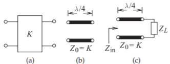
Figure \(\PageIndex{1}\): Inverter equivalence: (a) two-port impedance inverter (of impedance \(K\)): (b) a quarter-wave transmission line of characteristic impedance \(Z_{0} = K\); and (c) a terminated one-quarter wavelength long line.
called the impedance of the inverter. For an admittance inverter \(J\) is used and is called the characteristic admittance of the inverter, and sometimes just the admittance of the inverter. They are related as \(J = 1/K\). In Section 2.4.6 of [10] it is shown that a \(\lambda/4\) long line with a load has an input impedance that is the inverse of the load, normalized by the square of the characteristic impedance of the line. So an inverter can be realized at microwave frequencies using a one-quarter wavelength long transmission line (see Figure \(\PageIndex{1}\)(b)). For the configuration shown in Figure \(\PageIndex{1}\)(c),
\[\label{eq:2}Z_{\text{in}}=\frac{K^{2}}{Z_{L}} \]
2.8.1 Properties of an Impedance Inverter
An impedance inverter has the \(ABCD\) matrix
\[\label{eq:3}\mathbf{T}=\left[\begin{array}{cc}{0}&{\jmath K} \\ {\jmath /K}&{0}\end{array}\right] \]
where \(K\) is called the characteristic impedance of the inverter. With a load impedance, \(Z_{L}\) (at Port \(\mathsf{2}\)), the input impedance (at Port \(\mathsf{1}\)) is (as expected)
\[\label{eq:4}Z_{\text{in}}(s)=\frac{AZ_{L}+B}{CZ_{L}+D}=\frac{\jmath K}{(\jmath /K)Z_{L}}=\frac{K^{2}}{Z_{L}} \]
Now the \(ABCD\) matrix of the transmission line of Figure \(\PageIndex{1}\)(b) is
\[\label{eq:5}\left[\begin{array}{cc}{\cos\theta}&{\jmath Z_{0}\sin\theta} \\ {(\jmath /Z_{0})\sin\theta}&{\cos\theta}\end{array}\right] \]
which is identical to Equation \(\eqref{eq:3}\) when the electrical length is \(\theta = π/2\) (i.e., when the line is \(\lambda/4\) long). The inverter is shown in Figure 2.7.4(a) as a two-port and its implementation as a \(\lambda /4\) long line is shown in Figure 2.7.4(c). The bandwidth over which the line realizes an impedance inverter is limited, however, as it is an ideal inverter only at the frequency at which it is \(\lambda /4\) long.
2.8.2 Replacement of a Series Inductor by a Shunt Capacitor
A series inductor can be replaced by a shunt capacitor surrounded by a pair of inverters followed by a negative unity transformer (i.e., an inverter with \(K = 1\)). This equivalence is shown in Figure \(\PageIndex{2}\) and this will now be shown mathematically.
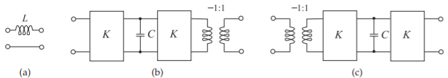
Figure \(\PageIndex{2}\): Equivalent realizations of a series inductor: (a) as a two-port; (b) its realization using a capacitor, inverters of characteristic impedance \(K\), and a negative unity transformer; and (c) an alternative realization. \(C = L/K^{2}\).
From Table 2.4.1 of [11], the \(ABCD\) matrix of the series inductor shown in Figure \(\PageIndex{2}\)(a) (which has an impedance of \(sL\)) is
\[\label{eq:6}\mathbf{T}_{L}=\left[\begin{array}{cc}{1}&{sL}\\{0}&{1}\end{array}\right] \]
and the \(ABCD\) matrix of the shunt capacitor (which has an admittance of \(sC\)) is, from Table 2.4.1 of of [11],
\[\label{eq:7}\mathbf{T}_{1}=\left[\begin{array}{cc}{1}&{0} \\ {sC}&{1}\end{array}\right] \]
The \(ABCD\) matrix of an inverter with \(K\) in ohms (generally the unit is dropped and ohms is assumed) is
\[\label{eq:8}\mathbf{T}_{2}=\left[\begin{array}{cc}{0}&{\jmath K} \\ {\jmath /K}&{0}\end{array}\right] \]
and finally, the \(ABCD\) matrix of a negative unity transformer, \(n = −1\), is, from Table 2.4.1 of [11],
\[\label{eq:9}\mathbf{T}_{3}=\left[\begin{array}{cc}{-1}&{0}\\{0}&{-1}\end{array}\right] \]
Then the \(ABCD\) matrix of the cascade shown in Figure \(\PageIndex{2}\)(b) is
\[\begin{align} \mathbf{T}_{C}&=\mathbf{T}_{2}\mathbf{T}_{1}\mathbf{T}_{2}\mathbf{T}_{3}\nonumber \\ &=\left[\begin{array}{cc}{0}&{\jmath K}\nonumber \\ {\jmath /K}&{0}\end{array}\right]\left[\begin{array}{cc}{1}&{0}\\{sC}&{1}\end{array}\right]\left[\begin{array}{cc}{0}&{\jmath K}\\{\jmath /K}&{0}\end{array}\right]\left[\begin{array}{cc}{-1}&{0}\\{0}&{-1}\end{array}\right] \nonumber \\ & =\left[\begin{array}{cc}{0}&{\jmath K}\\{\jmath /K}&{0}\end{array}\right]\left[\begin{array}{cc}{1}&{0}\\{sC}&{1}\end{array}\right]\left[\begin{array}{cc}{0}&{-\jmath K} \\ {-\jmath /K}&{0}\end{array}\right] \nonumber \\ &=\left[\begin{array}{cc}{\jmath sCK}&{\jmath K}\\{\jmath /K}&{0}\end{array}\right]\left[\begin{array}{cc}{0}&{-\jmath K} \\{-\jmath /K}&{0}\end{array}\right] \nonumber \\ \label{eq:10}&=\left[\begin{array}{cc}{1}&{sCK^{2}}\\{0}&{1}\end{array}\right]\end{align} \]
Thus \(T_{C} = T_{L}\) if \(L = CK^{2}\) (compare Equations \(\eqref{eq:6}\) and \(\eqref{eq:10}\)). Thus a series inductor can be replaced by a shunt capacitor with an inverter before and after it and with a negative unity transformer. The unity transformer
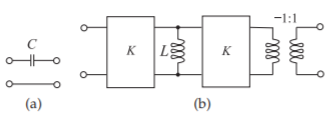
Figure \(\PageIndex{3}\): A series capacitor: (a) as a twoport; (b) its realization using a shunt inductor, inverters and negative unity transformer’ \(L = CK^{2}\).
may also be placed at the first port, as in Figure \(\PageIndex{2}\)(c). Thus the two-ports shown in Figure \(\PageIndex{2}\) are all electrically identical, with the limitation being the frequency range over which the inverter can be realized. An interesting and important observation is that as a result of the characteristic impedance of the inverter (e.g., \(50\:\Omega\)), a small shunt capacitor can be used to realize a large series inductance value.
Example \(\PageIndex{1}\): Inductor Synthesis Using an Inverter
Consider the network of Figure \(\PageIndex{2}\)(c) with inverters having a characteristic impedance of \(50\:\Omega\). What value of inductance is realized using a \(10\text{ pF}\) capacitor?
Solution
\(K = 50\), so \(L = CK^{2} = 10^{−11}\cdot 2500 = 25\text{ nH}\).
2.8.3 Replacement of a Series Capacitor by a Shunt Inductor
A series capacitor can be replaced by a shunt inductor plus inverters and a negative transformer (see Figure \(\PageIndex{3}\)). The \(ABCD\) parameters of the series capacitor in Figure \(\PageIndex{3}\)(a) are
\[\label{eq:11}\mathbf{T}=\left[\begin{array}{cc}{1}&{1/sC}\\{0}&{1}\end{array}\right] \]
and here it is shown that the cascade in Figure \(\PageIndex{3}\)(b) has the same \(ABCD\) parameters. The cascade in Figure \(\PageIndex{3}\)(b) has the \(ABCD\) parameters
\[\begin{align}\mathbf{T}&=\left[\begin{array}{cc}{0}&{\jmath K}\\{\jmath /K}&{0}\end{array}\right]\left[\begin{array}{cc}{1}&{0}\\{1/sL}&{1}\end{array}\right]\left[\begin{array}{cc}{0}&{\jmath K}\\{\jmath /K}&{0}\end{array}\right]\left[\begin{array}{cc}{-1}&{0}\\{0}&{-1}\end{array}\right]\nonumber \\ &=\left[\begin{array}{cc}{0}&{\jmath K}\\{\jmath /K}&{0}\end{array}\right]\left[\begin{array}{cc}{1}&{0}\\{1/sL}&{1}\end{array}\right]\left[\begin{array}{cc}{0}&{-\jmath K}\\{-\jmath /K}&{0}\end{array}\right] \nonumber \\ &=\left[\begin{array}{cc}{\jmath K/sL}&{\jmath K}\\{\jmath /K}&{0}\end{array}\right]\left[\begin{array}{cc}{0}&{-\jmath K}\\{-\jmath /K}&{0}\end{array}\right] \nonumber \\ \label{eq:12}&=\left[\begin{array}{cc}{1}&{K^{2}/sL}\\{0}&{1}\end{array}\right]\end{align} \]
So the series capacitor, \(C\), can be realized using a shunt inductor, \(L\), inverters, and a negative unity transformer, and \(C = L/K^{2}\). It is unlikely that this transformation would be exploited, as much better lower-loss capacitors can be realized at RF than inductors.
2.8.4 Ladder Prototype with Impedance Inverters
The transformations discussed in the previous two sections can be used to advantage in simplifying filters. In this section the transformations are
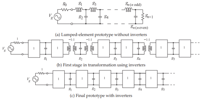
Figure \(\PageIndex{4}\): Ladder prototype filters using impedance inverters: (a) lumped-element prototype; (b) first stage in transformation using inverters; and (c) final stage.
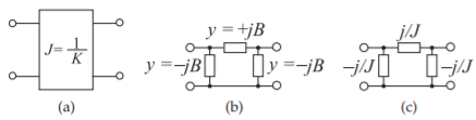
Figure \(\PageIndex{5}\): Admittance inverter: (a) as a two-port; (b) realized using lumped elements with \(B = −J\); and (c) lumped equivalent circuit (the element values in (c) are impedances).
applied to the prototype lowpass ladder filter shown in Figure \(\PageIndex{4}\)(a). The inductors in the ladder circuit are a particular problem as they have considerable resistance at microwave frequencies. The series inductors can be replaced by a circuit with capacitors, inverters, and transformers, as shown in Figure \(\PageIndex{4}\)(b). This simplifies further to the realization shown in Figure \(\PageIndex{4}\)(c), as the negative unity transformers only affect the phase of the transmission coefficient. So a lowpass ladder filter can be realized using just capacitors and inverters.
2.8.5 Lumped-Element Realization of an Inverter
The admittance inverter is functionally the same as the impedance inverter (see Figure 2.7.4(a)) and the schematic is the same (see Figure \(\PageIndex{5}\)(a)). As will be shown, an inverter can be realized using frequency-invariant lossless elements (i.e., elements whose reactance or susceptance do not vary with frequency) using the network of Figure \(\PageIndex{5}\)(b). Recall that \(J\) is used to identify an admittance inverter and \(K\) identifies an impedance inverter. If not specified by the context, the inverter (with value specified by a number) defaults to being an impedance inverter. Alternatively units can be used to indicate which type of inverter is being used. The function of
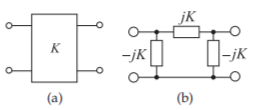
Figure \(\PageIndex{6}\): Impedance inverter: (a) as a two-port; and (b) its lumped equivalent circuit (the element values in (b) are impedances).
the inverter is the same in any case; both can be realized by one-quarter wavelength long lines, for example. For the remainder of this chapter it will be more convenient, most of the time, to use the admittance inverter, as many calculations will be in terms of admittances since most lumped elements in filters synthesis will be in shunt.
Now it will be shown that the lumped-element network of Figure \(\PageIndex{5}\)(b) realizes an inverter. To do this the inverter and the lumped-element network must have the same two-port parameters. First, the \(ABCD\) matrix of an inverter of characteristic admittance \(J\) is
\[\label{eq:13}\mathbf{T}_{j}=\left[\begin{array}{cc}{0}&{\jmath /J}\\{\jmath J}&{0}\end{array}\right] \]
Referring to Table 2-1 of [11], the circuit of Figure \(\PageIndex{5}\)(b) has the \(ABCD\) matrix
\[\begin{align}T&=\left[\begin{array}{cc}{1}&{0}\\{-\jmath B}&{1}\end{array}\right]\left[\begin{array}{cc}{1}&{1/(\jmath B)}\\{0}&{1}\end{array}\right]\left[\begin{array}{cc}{1}&{0}\\{-\jmath B}&{1}\end{array}\right]\nonumber \\ \label{eq:14}&=\left[\begin{array}{cc}{1}&{1/(\jmath B)}\\{-\jmath B}&{0}\end{array}\right]\left[\begin{array}{cc}{1}&{0}\\{-\jmath B}&{1}\end{array}\right]=\left[\begin{array}{cc}{0}&{-\jmath /B}\\{-\jmath B}&{0}\end{array}\right]\end{align} \]
where \(B\) is the susceptance of the frequency-invariant elements. Equation \(\eqref{eq:14}\) is identical to Equation \(\eqref{eq:13}\) if \(B = −J\). More practical equivalents of the circuit of Figure \(\PageIndex{5}\)(b) can be derived, as shown later.
For completeness, the lumped-element equivalent of the impedance inverter is shown in Figure \(\PageIndex{6}\) (derived from Figure \(\PageIndex{5}\) with \(J = 1/K\)).
Example \(\PageIndex{2}\): Lumped Inverter Analysis
Demonstrate that Figure \(\PageIndex{5}\)(b) is a lumped-element admittance inverter.
Solution
Terminating the network in Figure \(\PageIndex{5}\)(b) results in the network shown in Figure \(\PageIndex{7}\)(a). This is relabeled in Figure \(\PageIndex{7}\)(b), where the elements are admittances. Then
\[\label{eq:15}y_{\text{in}}=y_{3} // (y_{1}$(y_{2}+y_{L})) \]
where \(//\) indicates “in parallel with” and \($\) indicates “in series with.” These are common shorthand notations in circuit calculations. Continuing on from Equation \(\eqref{eq:15}\),
\[\label{eq:16}y_{\text{in}}=y_{3}+\left[\frac{1}{y_{1}}+\left(\frac{1}{y_{2}+y_{L}}\right)\right]^{-1}=y_{3}+\left[\frac{y_{2}+y_{L}+y_{1}}{y_{1}(y_{2}+y_{L})}\right]^{-1} \]
Substituting \(y_{1} =\jmath B\) and \(y_{2} = y_{3} = −\jmath B\), this becomes
\[\label{eq:17}y_{\text{in}}=-\jmath B+\frac{\jmath B(y_{L}-\jmath B)}{y_{L}}=\frac{-\jmath By_{L}+\jmath By_{L}+B^{2}}{y_{L}}=\frac{B^{2}}{y_{L}} \]
Thus the lumped-element circuit of Figure \(\PageIndex{5}\)(b) is a lumped-element admittance inverter of value \(B\) (in siemens).
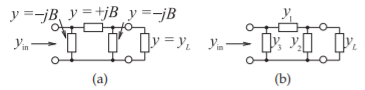
Figure \(\PageIndex{7}\): Terminated lumped-element admittance inverter.
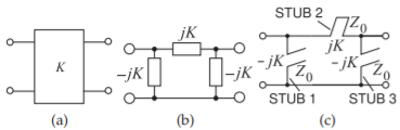
Figure \(\PageIndex{8}\): Narrowband inverter equivalents at frequency \(f_{0}\): (a) impedance inverter with characteristic impedance \(K\); (b) lumped-element equivalent network; and (c) inverter realized by short- and open-circuited stubs.
2.8.6 Narrowband Realization of an Inverter Using Transmission Line Stubs
In this section it will be shown that an impedance inverter can be implemented using short- and open-circuited stubs. The match is good over a narrow band centered at frequency \(f_{0}\). An impedance inverter is shown in Figure \(\PageIndex{8}\)(a) and its equivalent lumped-element network is shown in Figure \(\PageIndex{8}\)(b). A stub-based implementation is shown in Figure \(\PageIndex{8}\)(c), where there are short- and open-circuited stubs of characteristic impedance \(Z_{0}\). The input impedance of the stubs is shown at the inputs of the stubs. The stubs have an electrical length \(\theta\) at \(f_{0}\) and the stubs are one-quarter wavelength long (i.e., resonant) at what is called the commensurate frequency, \(f_{r}\).
Now it will be shown that the network of Figure \(\PageIndex{8}\)(c) is a good representation of the inverter at \(f_{0}\). This is done by matching \(ABCD\) parameters. The \(ABCD\) parameter matrix of an inverter is
\[\label{eq:18} T=\left[\begin{array}{cc}{0}&{\jmath K}\\{\jmath /K}&{0}\end{array}\right] \]
and, at frequency \(f_{0}\), the \(ABCD\) parameter matrix of the stub circuit of Figure \(\PageIndex{8}\)(c) is
\[\begin{align}T&=\left[\begin{array}{cc}{1}&{0}\\{-1/[\jmath Z_{0}\tan(\theta)]}&{1}\end{array}\right]\left[\begin{array}{cc}{1}&{\jmath Z_{0}\tan(\theta)}\\{0}&{1}\end{array}\right]\left[\begin{array}{cc}{1}&{0}\\{-1/[\jmath Z_{0}\tan (\theta)]}&{1}\end{array}\right] \nonumber \\ &=\left[\begin{array}{cc}{1}&{\jmath Z_{0}\tan(\theta)}\\{-1/[\jmath Z_{0}\tan(\theta)]}&{0}\end{array}\right]\left[\begin{array}{cc}{1}&{0}\\{-1/[\jmath Z_{0}\tan(\theta)]}&{1}\end{array}\right] \nonumber \\ \label{eq:19}&=\left[\begin{array}{cc}{0}&{\jmath Z_{0}\tan(\theta)}\\{\jmath /[Z_{0}\tan(\theta)]}&{0}\end{array}\right]\end{align} \]
Thus, equating Equations \(\eqref{eq:18}\) and \(\eqref{eq:19}\), the stub network is a good representation of the inverter if
\[\label{eq:20}K=Z_{0}\tan(\theta) \]
and so the required characteristic impedance of each stub at frequency \(f_{0}\) is
\[\label{eq:21}Z_{0}=\frac{K}{\tan(\theta)} =\frac{K}{\tan\left(\frac{\pi}{2}\frac{f_{0}}{f_{r}}\right)} \]
Special Case, \(f_{r}=2f_{0}\)
In most designs the stub resonant frequency, \(f_{r}\) (also called the commensurate frequency), is chosen to be twice that of the center frequency of the design, \(f_{0}\). So with \(f_{r} = 2f_{0}\), then at \(f_{0}\)
\[\label{eq:22}Z_{0}=\frac{K}{\tan\left(\frac{\pi}{2}\frac{f_{0}}{2f_{0}}\right)}=\frac{K}{\tan\pi /4}=K \]
and the input impedance of the stub is \(\jmath K\). So the characteristic impedance of the transmission line stub is \(Z_{0} = K\).