
2.14: Inter-resonator Coupled Bandpass Filters
- Page ID
- 46076
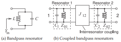
Figure \(\PageIndex{1}\): Bandpass resonators.
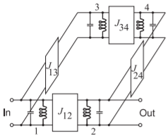
Figure \(\PageIndex{2}\): The electrical design of a cross-coupled filter. There are four resonators labeled \(\mathsf{1, 2, 3,}\) and \(\mathsf{4}\). The bandpass resonators are coupled by admittance inverters.
The synthesis method that has been described so far leads to bandpass filters that are a cascade of coupled bandpass resonators. A bandpass filter then comprises pairs of resonators of the type shown in Figure \(\PageIndex{1}\)(a) that are coupled using what is called inter-resonator coupling (see Figure \(\PageIndex{1}\)(b)). A generalization of this architecture is that a bandpass filter comprises coupled resonators that do not need to be in a linear cascade. Coupling the output of one resonator latter in a cascade to the input of an earlier resonator is called cross coupling, and a filter that uses this arrangement is said to be a crosscoupled resonator filter or a cross-coupled filter. By reusing resonators in this way, fewer resonators are required to achieve a specified bandpass response and the filter can have higher performance or be smaller. An example of the electrical design of a cross-coupled filter is shown in Figure \(\PageIndex{2}\).
Design of a cross-coupled bandpass filter is not as systematic as the design of a ladder filter. The design concept is based on using a number of resonators where each resonator on its own has the same resonant
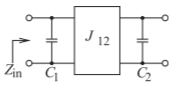
Figure \(\PageIndex{3}\): Lowpass filter approximation with capacitors separated by an admittance inverter.
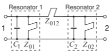
Figure \(\PageIndex{4}\): Segment of a filter with two resonators. \(C_{1} = C_{2} = 2.7171\text{ pF},\: Z_{01} = Z_{02} = 67.7535\:\Omega\), and \(Z_{012} = 442.3836\:\Omega\). The stubs are resonant at \(f_{r} = 2f_{0}\) where the filter center frequency \(f_{0} = 1\text{ GHz}\). Thus the stubs are \(\lambda /8\) long at \(f_{0}\).
frequency \(f_{0}\), where \(f_{0}\) is the center frequency of the filter. The desired filter characteristics are obtained by adjusting the inter-resonator coupling, that is, the coupling between pairs of resonators. Design is not a synthesis process based on a series of mathematical transformations, but instead is based on the understanding of the impact of changing the coupling. The design process will now be described for a pair of resonators.
Coupling of a Pair of Resonators
A segment of a bandpass filter fundamentally comprises a pair of coupled bandpass resonators. This is based on the lowpass prototype with a pair of capacitors separated by an admittance inverter (see Figure \(\PageIndex{3}\)). In transforming this to a bandpass filter with a center frequency of \(f_{0}\), each capacitor is replaced by a resonator such as that shown in Figure \(\PageIndex{1}\)(a). This leads to a pair of resonators, each resonant at \(f_{0}\), that are coupled by an inverter (see Figure \(\PageIndex{1}\)(b)). The value of the inverter determines the level of coupling of the resonators.
Consider the circuit in Figure \(\PageIndex{4}\), which consists of a pair of coupled resonators, with each resonator resonant at \(f_{0} = 1\text{ GHz}\), and the resonators are coupled by the series stub with characteristic impedance \(Z_{012}\) (i.e., the \(Z_{012}\) stub). The circuit of Figure \(\PageIndex{4}\) is a segment of a Chebyshev \(1\text{ GHz}\) bandpass filter with a fractional bandwidth of \(10\%\). This is an interim stage of a bandpass filter design\(^{1}\) and the system impedance of this circuit segment is \(139.4\:\Omega\). The magnitude and phase of the \(139.4-\Omega\: S_{21}\) and \(S_{11}\) parameters of this circuit are shown in Figure \(\PageIndex{5}\)(a), and the phase of \(S_{21}\) is shown in Figure \(\PageIndex{5}\)(b). Specific features to identify here are the two peaks in the phase response at \(f_{1}\) and \(f_{2}\). These are also the frequencies of peak transmission response where \(|S_{21}| = 1\). The bandwidth defined by \(f_{1}\) and \(f_{2}\) is called the coupling bandwidth \((= f_{2} − f_{1})\) or the bandwidth of the filter (note that this is not the \(3\text{-dB}\) bandwidth of the filter). The level of coupling determines the coupling bandwidth. That is, changing the level of coupling provided by the \(Z_{012}\) stub changes the position of \(f_{1}\) and \(f_{2}\). An interpretation of what is happening is that by coupling the two resonators, the resonate frequency of the resonators on their own, \(f_{0}\), has been split by the coupling, resulting in two peaks at \(f_{1}\) and \(f_{2}\). The higher the coupling, the larger the coupling bandwidth, and the lower the coupling, the smaller the coupling bandwidth. For example, a narrowband bandpass filter comprises
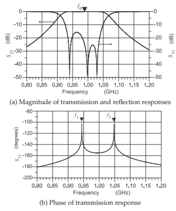
Figure \(\PageIndex{5}\): Response of the coupled resonator network in Figure \(\PageIndex{4}\).
resonators that have low-level coupling.
So following the choice of an appropriate architecture, that is, the number of resonators and the coupling arrangement, design and manual optimization becomes one of changing the level of coupling between pairs of resonators. Design is not as clean as for ladder filters, but the advantages of a design with fewer resonators is a compelling justification. Invariably, extensive (perhaps a day’s worth) manual adjustment of the coupling of the final fabricated filter is required. Overall this is an approach worth adopting for high-value filters such as those used in a basestation, where the high unit costs resulting from manual tuning of individual filters can be justified. This type of filter design is considered further in [3, 18, 19, 20, 21].
Relationship of Ladder Synthesis and Inter-resonator Coupling
The relationship of design focused on interresonator coupling and design based on the ladder synthesis approach can be demonstrated for a pair of resonators as follows. Consider the lowpass prototype circuit of Figure \(\PageIndex{3}\). The input impedance of this circuit is
\[\label{eq:1}Z_{\text{in}}(s)=[sC_{1}+J_{12}^{2}/(sC_{2})]^{-1} \]
With \(s =\jmath\omega\), the poles of \(Z_{\text{in}}\) occur when
\[\label{eq:2}J_{12}^{2}-\omega^{2}C_{1}C_{2}=0 \]
thus the radian frequencies of the poles are
\[\label{eq:3}\omega =\pm\frac{J_{12}}{\sqrt{C_{1}C_{2}}} \]
Applying the bandpass transformation (so that the capacitors are replaced by the resonators of Figure \(\PageIndex{1}\)(a)) results in the bandpass circuit of Figure \(\PageIndex{1}\)(b). With this transformation the frequency is transformed as
\[\label{eq:4}\omega\to\alpha\left(\frac{\omega}{\omega_{0}}-\frac{\omega_{0}}{\omega}\right) \]
That is, the transmission coefficient of the bandpass filter is
\[\label{eq:5}T_{\text{BPF}}(\omega)=T_{\text{LPF}}\left(\alpha\left[\frac{\omega}{\omega_{0}}-\frac{\omega_{0}}{\omega}\right]\right) \]
where \(T_{\text{LPF}}(\omega )\) is the transmission coefficient of the lowpass filter at the radian frequency \(\omega\). The poles of the bandpass filter are at \(\omega_{1}\), where
\[\label{eq:6}\alpha\left(\frac{\omega_{1}}{\omega_{0}}-\frac{\omega_{0}}{\omega_{1}}\right)=+\frac{J_{12}}{\sqrt{C_{1}C_{2}}} \]
and \(\omega_{2}\), where
\[\label{eq:7}\alpha\left(\frac{\omega_{2}}{\omega_{0}}-\frac{\omega_{0}}{\omega_{2}}\right)=-\frac{J_{12}}{\sqrt{C_{1}C_{2}}} \]
Then the coupling bandwidth of the filter is
\[\label{eq:8}f_{1}-f_{2}=\frac{\omega_{1}-\omega_{2}}{2\pi}=\frac{J_{12}\omega_{0}}{2\pi\alpha\sqrt{C_{1}C_{2}}} \]
Thus the coupling bandwidth can be directly related to the steps in the ladder-based synthesis of a bandpass ladder filter.
Group Delay
Group delay of a network, and in particular of a filter, is the delay to send information through a network. It is the time required for a modulated carrier signal to appear at the output of a filter after being applied to the input of the filter. Phase delay is a similar measure of delay but does not describe the time it takes to send information. It describes the delay to send a particular phase of a single sinewave. Group delay is a steady-sate concept and so only approximately captures the transient response of a filter.
If a two-port has the transmission coefficient
\[\label{eq:9}T(s)=S_{21}=a+\jmath b=t\angle\varphi \]
where \(a\) and \(b\) are its real and imaginary parts, \(t\) is its magnitude, and \(\varphi\) is its phase. With \(s =\jmath\omega\), the phase of \(T\) is
\[\label{eq:10}\varphi(\omega)=\tan^{-1}\left(\frac{b}{a}\right) \]
The group delay, \(\tau_{D}\), is the negative of the derivative of this phase as follows:
\[\label{eq:11}\text{Group delay }=\tau_{g}(\omega)=-\frac{d\varphi}{d\omega}=-\frac{d}{d\omega}\left[\tan^{-1}\left(\frac{b}{a}\right)\right] \]
This compares to the phase delay:
\[\label{eq:12}\text{Phase delay }=\tau_{\varphi}(\omega)=-\frac{\varphi}{\omega}=-\tan^{-1}\left(\frac{b}{a}\right) \]
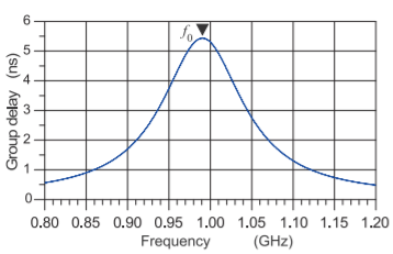
Figure \(\PageIndex{6}\): Group delay of a resonator.
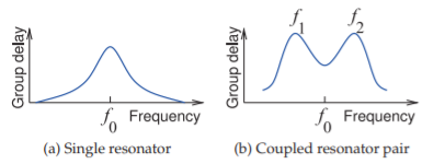
Figure \(\PageIndex{7}\): Group delay of resonators in a filter. Additional delay is introduced by the coupling inverter.
Figure \(\PageIndex{6}\)(c) shows the group delay response of one of the resonators in Figure \(\PageIndex{4}\), where the group delay peaks at the resonant frequency of the resonator \(f_{0}\). The peak of the group delay occurs at the resonant frequency of the resonator without loading. From examination of the phase of \(S_{21}\) (see Figure \(\PageIndex{5}\)(b)), it is clear that the group delay peaks very close to \(f_{1}\) and \(f_{2}\). So the coupled resonator pair has two peaks in the group delay. This can be seen in Figure \(\PageIndex{7}\), which plots the group delay of a single resonator and a coupled pair of resonators.
Footnotes
[1] Specifically these resonators are the left-most resonators in a design developed in Chapter 3 (see Figure 3.4.16).