
3.4: Case Study- Third-Order Chebyshev Combline Filter Design
- Page ID
- 46110
Example \(\PageIndex{1}\): Inductor Synthesis
Lumped inductors have low \(Q\). Fortunately, in microwave design they can be realized using inverters and a shunt capacitor that have a high \(Q\). Realize the series inductor in Figure \(\PageIndex{1}\)(a) with a shunt capacitor and \(10\:\Omega\) impedance inverters.
Solution
The series inductor in a \(1\:\Omega\) system is transformed into a network with inverters and a shunt capacitor using the transformation shown in Figure 2.13.3. Thus here the series inductor can be realized by the circuit of Figure \(\PageIndex{1}\)(b), where the shunt capacitor \(C\) has the same numeric value as the series inductor. The inverters here can be either impedance inverters or admittance inverters, as their value is equal to one. The design requires that these be realized as \(10\:\Omega\) inverters, but scaling is performed on admittance inverters, as shown in Figure \(\PageIndex{1}\)(c), where the value of the admittance inverters is \(0.1\text{ S }=\sqrt{x}\). Thus \(x = 0.01\) and the admittance of the capacitor is scaled by \(0.01\), so \(C_{1} = C/100 = 10\text{ pF}\). The final design is shown in Figure \(\PageIndex{1}\)(d).
This section presents the design of a \(1\text{ GHz}\) third-order Chebyshev combline bandpass filter with \(10\%\) bandwidth. The combline filter is one of the most commonly used transmission line-based filters and uses the combline section shown in Figure 3.2.13. The synthesis that will be presented here combines many of the concepts discussed previously in this chapter. There are also design decisions that must be made in response to particular situations encountered during synthesis. An example of a design decision is deciding what to do if the characteristic impedance of a transmission line is too low.
Step 1: Choice of Lowpass Filter Prototype
Design begins with the choice of a prototype that is expected to achieve the required specifications. If the choice is eventually found to be not suitable, then another topology must be chosen and the synthesis restarted. Consider a third-order Chebyshev lowpass filter prototype, shown in Figure \(\PageIndex{2}\), with a passband ripple factor of \(\varepsilon = 0.1\) (or \(0.043\text{ dB}\)). The element values were calculated using Equations (2.7.6)–(2.7.13). Note that at the corner frequency that defines the bandwidth of the lowpass filter, the square of the transmission coefficient is the ripple level (see Figure 2.5.1). That is, at frequency \(\omega_{0} = 1\text{ rad/s}\), the squared transmission coefficient is \(1/(1 + \varepsilon^{2})\) (or in decibels the ripple is \(R_{\text{dB}} = 10 \log(1 + \varepsilon^{2})\)).
Step 2: Replace Series Elements
The next step in the transformation of the lowpass prototype in Figure \(\PageIndex{2}\) is replacing the series inductor by a shunt capacitor in cascade with admittance inverters, as shown in Figure \(\PageIndex{3}\). This step uses the series inductor transformation shown in Figure \(\PageIndex{1}\).
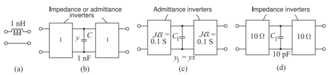
Figure \(\PageIndex{1}\): Realization of a series inductor as a shunt capacitor with inverters.
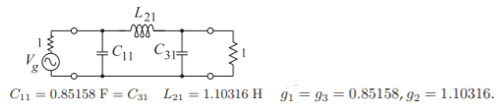
Figure \(\PageIndex{2}\): Step 1. A third-order Chebyshev lowpass filter prototype.
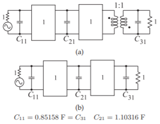
Figure \(\PageIndex{3}\): Step \(2\). Prototype filter with inductor replaced by a capacitor and admittance inverter combination: (a) with a unity inverting transformer; and (b) with the transformer eliminated as it shifts the transmission phase by \(180^{\circ}\) and so has no effect on the filter response. Note that \(|C_{21}| = |L_{21}|\).
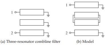
Figure \(\PageIndex{4}\): Target combline filter physical layout.
Step 3: Bandpass Filter Transformation
In synthesizing the bandpass filter the final physical topology must be considered. The essential element of a third-order combline filter comprises three coupled lines as shown in Figure \(\PageIndex{4}\)(a). The three resonators can be modeled as two pairs of coupled lines, as shown in Figure \(\PageIndex{4}\)(b), with one line shared by each pair. Each pair of coupled lines can be modeled by a Pi network of stubs as shown in Figure 3.2.14(b). Thus the lowpass prototype of Figure \(\PageIndex{3}\)(b) needs to be converted to a bandpass filter and eventually this needs to be transformed into two cascaded Pi networks of stubs.
In this step the prototype is converted to a bandpass circuit. The filter has 10% bandwidth with approximate corner frequencies at \(f_{1} = 950\text{ MHz}\) and \(f_{2} = 1050\text{ MHz}\). Using the filter type transformations in Figure 2.9.5, \(\omega_{0} = 2\pi 10^{9}\), and \(\alpha =\omega_{0}/(\omega_{2} −\omega_{1}) = 1/(\text{fractional bandwidth}) = 10\), the first capacitor in Figure \(\PageIndex{3}\), \(C_{11}\), is transformed to
\[\label{eq:1}C_{1}'=\frac{\alpha C_{11}}{\omega_{0}}=1355.33\text{ pF}\quad\text{in parallel with }\quad L_{1}'=\frac{1}{\alpha C_{11}\omega_{0}}=0.0186894\text{ nH} \]
The other capacitors are transformed similarly and the bandpass prototype becomes that shown in Figure \(\PageIndex{5}\).
The lumped-element version of the bandpass filter is shown in Figure \(\PageIndex{6}\) along with its simulated response. This response is the ideal electrical response and provides a reference in design. Note that the ripples in the transmission response, i.e. \(S_{21}\), are not evident on this scale. Losses in the implemented filter will smooth the ripples even further although the poles in the \(S_{21}\) response are not evident, these correspond to the zeros in the \(S_{11}\) response and these are clearly visible. Figure \(\PageIndex{6}\) shows three zeros in the \(S_{11}\) response, as expected for a third-order filter.
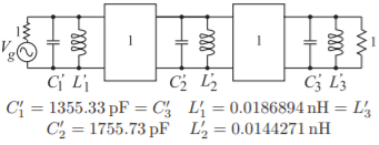
Figure \(\PageIndex{5}\): Step 3. Bandpass filter prototype with inverters derived from the lowpass filter prototype of Figure \(\PageIndex{3}\).
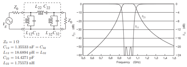
Figure \(\PageIndex{6}\): A third-order lumped-element Chebyshev bandpass filter with \(10\%\) bandwidth, ripple factor of \(\varepsilon = 0.1\), and center frequency of \(1\text{ GHz}\). The \(S\) parameters are referenced to \(1\:\Omega\).
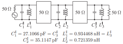
Figure \(\PageIndex{7}\): Step 4. Bandpass filter approximation where the inverters are now impedance inverters.
Step 4: Impedance Scaling
The system impedance is now scaled from \(1\) to \(50\:\Omega\), leading to the prototype in Figure \(\PageIndex{7}\) (derived from Figure \(\PageIndex{5}\)).
Step 5: Conversion of Lumped-Element Resonators
Each lumped-element resonator in Figure \(\PageIndex{7}\) comprises a capacitor and an inductor. The inductors are particularly difficult to realize efficiently and have high loss. The idea is to replace each lumped resonator (e.g., \(C_{1}^{♯}\) and \(L_{1}^{♯}\) in Figure \(\PageIndex{7}\)) with a network comprising a lumped capacitor and a transmission line stub.
Equivalence of a Capacitively-Loaded Stub and an LC Resonator
Here it will be shown that a capacitively-loaded stub is a broadband approximation of a lumped \(LC\) resonator. The resonator equivalence is shown in Figure \(\PageIndex{8}\). The equivalence is first developed at frequency \(f_{0} = \omega_{0}/(2\pi )\) by making sure that the circuits have the same admittance at the
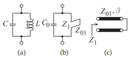
Figure \(\PageIndex{8}\): Resonator equivalence: (a) lumped resonator resonant at radian frequency \(\omega_{0}\); (b) mixed lumped-distributed resonator containing a short-circuited stub of characteristic impedance \(Z_{0}\) and resonant at radian frequency \(\omega_{r}\); and (c) short-circuited transmission line stub resonant at radian frequency \(\omega_{r}\). In (b) and (c) \(Z_{01}\) is the characteristic impedance of the transmission line and \(Z_{1}\) is the input impedance of the shorted transmission line.
filter center frequency. The broadband approximation is obtained by also equating the derivatives of the admittances at \(\omega_{0}\).
The input admittance of the parallel \(LC\) lumped-element resonator is
\[\label{eq:2}Y_{\text{in}}=\frac{\jmath(\omega^{2}LC-1)}{\omega L} \]
and has a radian frequency derivative of
\[\label{eq:3}\frac{dY_{\text{in}}}{d\omega}=\frac{\jmath(\omega^{2}LC+1)}{\omega^{2}L} \]
Now consider a short-circuited stub that is resonant at radian frequency \(\omega_{r}\); that is, the short-circuited stub is one-quarter wavelength long at \(\omega_{r}\).
From Equation (2.8.7) of [29], the input impedance at \(\omega\) is
\[\label{eq:4}Z_{1}=\jmath Z_{01}\tan\left(\frac{\pi}{2}\frac{\omega}{\omega_{r}}\right) \]
Thus for the lumped-distributed network in Figure \(\PageIndex{8}\)(b), the input admittance is
\[\label{eq:5}Y_{\text{in}}'=\frac{\jmath\left[\omega C_{0}Z_{01}\tan\left(\frac{\pi}{2}\frac{\omega}{\omega_{r}}\right)-1\right]}{Z_{01}\tan\left(\frac{\pi}{2}\frac{\omega}{\omega_{r}}\right)} \]
and its radian frequency derivative is
\[\label{eq:6}\frac{dY_{\text{in}}'}{d\omega}=\jmath\frac{1}{2}\left(\frac{\left\{2C_{0}Z_{01}\left[\tan\left(\frac{\pi}{2}\frac{\omega}{\omega_{r}}\right)\right]^{2}\omega\omega_{r}+\pi+\pi\left[\tan\left(\frac{\pi}{2}\frac{\omega}{\omega_{r}}\right)\right]^{2}\right\}}{Z_{01}\left[\tan\left(\frac{\pi}{2}\frac{\omega}{\omega_{r}}\right)\right]^{2}\omega_{r}}\right) \]
For the lumped-element and lumped-distributed resonators to be identical at \(\omega_{0}\) and approximating each other at nearby frequencies, Equations \(\eqref{eq:2}\) and \(\eqref{eq:5}\) are equated,
\[\label{eq:7}Y_{\text{in}}(\omega_{0})=Y_{\text{in}}'(\omega_{0}) \]
and Equations \(\eqref{eq:3}\) and \(\eqref{eq:6}\) are also equated,
\[\label{eq:8}\left.\frac{dY_{\text{in}}}{d\omega}\right|_{\omega=\omega_{0}}=\left.\frac{dY_{\text{in}}'}{d\omega}\right|_{\omega=\omega_{0}} \]
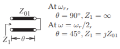
Figure \(\PageIndex{9}\): Short-circuited transmission line used as a stub resonator in a bandpass filter. The line is resonant at the radian frequency \(\omega_{r}\) and so the electrical length of the line is \(\theta = 90^{\circ}\). Using the design choice here, the filter center passband frequency \(\omega = \omega_{r}/2,\) and so \(\theta = 45^{\circ}\) and so the input impedance of the shorted stub is \(Z_{1} =\jmath Z_{01}\).
Specific Design Choice, \(\omega_{r}=2\omega_{0}\)
At this stage a design choice must be made regarding the relationship of \(\omega_{0}\) and \(\omega_{r}\); that is, the resonant frequency of the stub in relation to the resonant frequency of the resonator (which is also the center frequency of the filter passband). Here a shorted stub is considered that is resonant when it is \(\lambda /4\) long. The specific design choice made here is that the resonant frequency of the stub, \(f_{r}\), is twice the center frequency of the filter passband, i.e. \(\omega_{r} = 2\omega_{0}\). This is a common design choice. The consequence of this choice is illustrated in Figure \(\PageIndex{9}\). The frequency \(f_{r}\) is called the commensurate frequency to avoid confusion resulting from the resonant frequency of the filter resonators being different from the resonant frequency of stub\(^{1}\). The stub design proceeds as follows.
The equivalence expressed by Equations \(\eqref{eq:7}\) and \(\eqref{eq:8}\) is established at the center of the passband (i.e., at \(\omega_{0}\)). Now \(\omega =\omega_{0} =\frac{1}{2}\omega_{r}\), so Equations \(\eqref{eq:2}\), \(\eqref{eq:5}\), and \(\eqref{eq:7}\) become
\[\label{eq:9}\frac{\jmath\left[\left(\frac{\omega_{r}}{2}\right)^{2}Lc-1\right]}{\frac{\omega_{r}}{2}L}=\frac{\jmath\left[\frac{\omega_{r}}{2}C_{0}Z_{01}\tan\left(\frac{\pi}{2}\frac{\omega_{r}/2}{\omega_{r}}\right)-1\right]}{Z_{01}\tan\left(\frac{\pi}{2}\frac{\omega_{r}/2}{\omega_{r}}\right)} \]
That is,
\[\label{eq:10}\frac{(\omega_{r}^{2}LC-4)}{2\omega_{r}L}=\frac{\left[\frac{\omega_{r}}{2}C_{0}Z_{0}\tan(\pi/4)-1\right]}{Z_{01}\tan(\pi/4)} \]
Since \(\tan\frac{\pi}{4}=1\),
\[\label{eq:11}\frac{(\omega_{r}^{2}LC-4)}{2\omega_{r}L}=\frac{(\frac{1}{2}\omega_{r}C_{0}Z_{01}-1)}{Z_{01}} \]
and rearranging,
\[\label{eq:12}C_{0}=C-\frac{4}{\omega_{r}^{2}L}+\frac{2}{\omega_{r}Z_{01}} \]
Another relationship comes from equating derivatives. From Equations \(\eqref{eq:3}\), \(\eqref{eq:6}\), and \(\eqref{eq:8}\), and with \(\omega =\frac{1}{2}\omega_{r}\) and \(\tan(\frac{\pi}{2}\frac{\omega}{\omega_{r}}) = \tan\frac{\pi}{4} = 1\),
\[\label{eq:13}\frac{(\omega_{r}^{2}LC+4)}{\omega_{r}^{2}L}=\frac{1}{2}\frac{(2C_{0}Z_{01}\frac{1}{2}\omega_{r}^{2}+\pi+\pi)}{Z_{01}\frac{1}{2}\omega_{r}}=\frac{(C_{0}Z_{01}\omega_{r}^{2}+2\pi)}{Z_{01}\omega_{r}} \]
Substituting for \(C_{0}\) from Equation \(\eqref{eq:12}\) and rearranging, the characteristic impedance of the stub is
\[\label{eq:14}Z_{01}=\frac{\omega_{r}L}{4}\left(1+\frac{\pi}{2}\right) \]
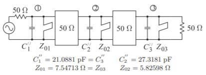
Figure \(\PageIndex{10}\): Step 5. Bandpass combline filter with impedance inverters. The transmission line stubs present impedances \(Z_{1} =\jmath Z_{01},\: Z_{2} = \jmath Z_{02}\), and \(Z_{3} = \jmath Z_{03}\) since the resonant frequencies of the stubs are twice that of the design center frequency, i.e. \(f_{r} = 2f_{0}\).
In the passband the input impedance of the stub is
\[\label{eq:15}Z_{1}=\jmath Z_{01}\tan(\beta\ell)=\jmath Z_{01}\tan(\pi /4)=\jmath Z_{01} \]
Thus the broadband \((\approx 30\%)\) approximation of the parallel LC resonant circuit is a capacitively-loaded stub, see Figure \(\PageIndex{8}\)(b), of length \(\lambda /8\) at the resonant frequency of the LC resonator. The resonant frequency of each stub, i.e. the frequency \(f_{r}\) at which they are \(\lambda /4\) long, is twice the design center frequency \(f_{0}\), i.e. \(f_{r} = 2f_{0}\). So the concept used here is that the resonant frequency of a stub does not need to be the same as the design center frequency. It is common for all the stubs in a design to have the same resonant frequency \(f_{r}\) and this is specified in the design documentation. In general \(f_{r}\) can have any relationship to \(f_{0}\) but the most common situation is \(f_{r} = 2f_{0}\) as used here.
Returning to Step 5
For this filter, the center of the passband is \(1\text{ GHz}\), and so \(\omega_{0} = 2\pi 10^{9}\) and \(\omega_{r} = 2\omega_{0} = 2\pi (2\cdot 10^{9})\) defines the stub resonant frequency as \(2\text{ GHz}\). The first resonator in Figure \(\PageIndex{7}\) with \(L = 0.934468\text{ nH}\) and \(C = 27.1066\text{ pF}\) can be replaced by the capacitively-loaded stub in Figure \(\PageIndex{8}\)(b). where, from Equation \(\eqref{eq:14}\),
\[\label{eq:16}Z_{01}=7.54713\:\Omega\quad\text{and from Equation }\eqref{eq:12},\quad C_{0}=21.0881\text{ pF} \]
This process is repeated for each lumped-element resonator in Figure \(\PageIndex{7}\), leading to the prototype shown in Figure \(\PageIndex{10}\).
Steps 6 and 7: Equating Characteristic Impedances of Stubs
The stubs in Figure \(\PageIndex{10}\) can be physically realized using transmission line segments. It would be ideal if the impedances of the stubs (i.e., the impedances looking into the stubs) are identical. To achieve this, the method of nodal admittance matrix scaling described in Section 3.3 is used with the impedance inverters multiplied by \(\sqrt{Z_{01}/Z_{02}}\) and the admittance, \(C_{2}′′ //Z_{2}\), divided by \(Z_{01}/Z_{02}\) (\(C_{2}′′\) is divided by \(Z_{01}/Z_{02}\), and \(Z_{2}\) is multiplied by \(Z_{01}/Z_{02}\)). This step scales each inverter impedance to \(56.9084\:\Omega\) and also sets the characteristic impedance of all the shunt stubs to \(7.54713\:\Omega\). The combline filter is now as shown in Figure \(\PageIndex{11}\).
In Section 2.8.6 it was shown that a good narrowband model of an inverter is a Pi network of stubs. So the inverter in the current filter design, shown in Figure \(\PageIndex{12}\)(a), is modeled by the lumped-element circuit in Figure \(\PageIndex{12}\)(b) and the stub circuit shown in Figure \(\PageIndex{12}\)(c).
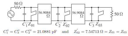
Figure \(\PageIndex{11}\): Step 6. Bandpass combline filter with impedance inverters with \(f_{r} = 2f_{0}\).
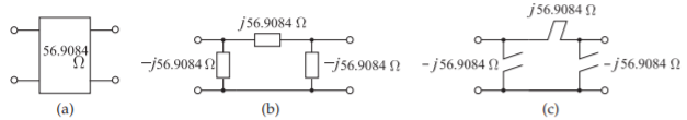
Figure \(\PageIndex{12}\): Inverter translation used with the combline filter design: (a) impedance inverter; (b) realization as a lumped-element circuit; and (c) realization using stubs resonant at twice the passband center frequency.
Stub Impedance When \(f_{r}=2f_{0}\)
The most common design choice is to select the resonant (i.e., the commensurate) frequency of the stubs to be twice the center frequency of the design. With \(f_{r} = 2f_{0}\), Equation (2.8.21) becomes
\[\label{eq:17}Z_{0}=\frac{1}{J\tan\left(\frac{\pi}{2}\frac{\omega_{0}}{2\omega_{0}}\right)}=\frac{1}{J\tan\left(\frac{\pi}{4}\right)}=\frac{1}{J}=K \]
Equation \(\eqref{eq:17}\) defines the characteristic impedance of the transmission line stubs realizing an inverter. Then the elements of the subnetwork in Figure \(\PageIndex{12}\)(b) all have the admittance magnitude
\[\label{eq:18}J=1/K=1/(56.9084\:\Omega)=17.5721\text{ mS} \]
and the stubs in Figure \(\PageIndex{12}\)(c) have the characteristic impedance
\[\label{eq:19}Z_{0}=\frac{1}{J\tan(\theta)}=\frac{K}{\tan(\theta)}=\left.\frac{K}{\tan\left(\frac{\pi}{2}\frac{\omega}{\omega_{r}}\right)}\right|_{\omega=\omega_{0}}=56.9084\:\Omega \]
At this stage there are several pairs of stubs in parallel. Figure \(\PageIndex{13}\) illustrates how a pair of parallel stubs can be replaced by a single stub. Now the prototype is as shown in Figure \(\PageIndex{14}\).
Step 8: Scaling Characteristic Impedances of Stubs
The filter will be realized using coupled microstrip lines and a general statement can be made about how the stubs in the prototype in Figure \(\PageIndex{14}\) correspond to the physical structure of the coupled lines. The stubs with characteristic impedances \(Z_{01}′, Z_{02}′′\), and \(Z_{03}′\) are largely realized by the properties of the individual microstrip lines. A low \(Z_{01}′\), for example, would
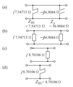
Figure \(\PageIndex{13}\): Step 6b. Procedure combining two parallel stubs to obtain one stub: (a) two parallel stubs; (b) represented as parallel impedances; (c) as one impedance; and (d) final representation as one stub. Note that the stubs must have the same commensurate frequency, i.e. they must have the same electrical length.
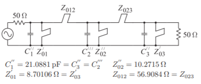
Figure \(\PageIndex{14}\): Step 7: Bandpass filter approximation where \(Z_{01}′,\: Z_{02}'',\: Z_{03}′,\: Z_{012}\), and \(Z_{023}\) are the characteristic impedances of the stubs with commensurate frequency \(f_{r} = 2f_{0}\).
require a wide microstrip line. The stubs with characteristic impedances \(Z_{012}\) and \(Z_{023}\) each correspond to coupling between pairs of microstrip lines with high impedances corresponding to low-level coupling and widely spaced microstrip lines.
In Figure \(\PageIndex{14}\) the short-circuited shunt stubs have characteristic impedances of \(8.7\:\Omega\) and \(10.3\:\Omega\), which are too low, and will result in wide microstrip lines.\(^{2}\) These need to be scaled to a higher impedance level to raise the characteristic impedances of the short-circuited stubs to an acceptable value. Note that the characteristic impedance of the middle shunt shortcircuited stub can be raised to \(80\:\Omega\) if the system impedance is raised from \(50\:\Omega\) to \(389.426\:\Omega\). Doing this leads to the element values shown in the bandpass circuit of Figure \(\PageIndex{15}\).
Step 9: Scaling to a \(50\:\Omega\) System Impedance
The previous step raised the system impedance (the required source and load impedances) to an unreasonably high level \((389.426\:\Omega)\). For the filter to operate in a \(50\:\Omega\) system, input and output impedance inverters are required to scale the source and load back to \(50\:\Omega\). The resulting circuit is shown in
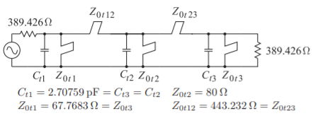
Figure \(\PageIndex{15}\): Step 8: Bandpass filter approximation.
Figure \(\PageIndex{16}\): Step 9: Bandpass filter approximation.
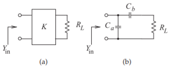
Figure \(\PageIndex{17}\): Inverter equivalence: (a) resistively-terminated impedance inverter; and (b) its equivalent capacitor network. Here \(Z_{\text{in}} = 1/Y_{\text{in}} = 389.426\:\Omega,\: R_{L} = 50\:\Omega,\) and \(K = 139.540\:\Omega\).
Figure \(\PageIndex{16}\) with input and output inverters of impedance \(\sqrt{50\times 389.426} = 139.540\:\Omega\).
3.4.1 Realization of the Input/Output Inverters
At this stage the design is as shown in Figure \(\PageIndex{16}\), where the inverters at the input and output remain to be synthesized. There are many possible realizations of the inverters. Focusing on just the output inverter with a load \(R_{L}\), as shown in Figure \(\PageIndex{17}\)(a), it will be shown here how this can be realized using the capacitive network of Figure \(\PageIndex{17}\)(b).
The input admittance of the inverter plus load resistor of Figure \(\PageIndex{17}\)(a) is
\[\label{eq:20}Y_{\text{in}}=\frac{R_{L}}{K^{2}} \]
and the input admittance of the circuit in Figure \(\PageIndex{17}\)(b) is
\[\label{eq:21}Y_{\text{in}}=sC_{a}+\frac{1}{1/(sC_{b})+R_{L}} \]
Thus, equating the real parts of Equations \(\eqref{eq:20}\) and \(\eqref{eq:21}\),
\[\label{eq:22}\Re (Y_{\text{in}})=\frac{R_{L}\omega^{2}C_{b}^{2}}{R_{L}^{2}\omega^{2}C_{b}^{2}+1}=\frac{R_{L}}{K^{2}} \]
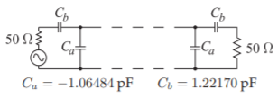
Figure \(\PageIndex{18}\): The external inverters of the prototype shown in Figure \(\PageIndex{16}\) replaced by capacitive networks.
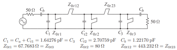
Figure \(\PageIndex{19}\): Step 10: The bandpass filter approximation combining the capacitive equivalent of the inverters with the first and last capacitors in the circuit of Figure \(\PageIndex{16}\).
and equating the imaginary parts yields
\[\label{eq:23}\Im (Y_{\text{in}})=\omega\left[C_{a}+\frac{C_{b}}{1+(\omega C_{b}R_{L})^{2}}\right]=0 \]
Thus
\[\label{eq:24}C_{b}=\frac{1}{\omega K\sqrt{1-R_{L}^{2}/K^{2}}},\quad C_{a}=\frac{-C_{b}}{1+(\omega C_{b}R_{L})^{2}} \]
and the inverters shown in Figure \(\PageIndex{16}\) can be replaced by the capacitive networks shown in Figure \(\PageIndex{18}\). This capacitive network is not a general replacement of an inverter. It only works when the inverter is terminated in a resistor. Note that \(C_{a}\) is negative, and this is absorbed in the first and last resonators so that the final lumped-distributed realization is as shown in Figure \(\PageIndex{19}\). This is the electrical design of the bandpass filter in a form that can be realized using the combline connection of coupled lines.
3.4.2 Implementation
The filter designed in the previous section can be implemented using three parallel microstrip lines, as shown in Figure \(\PageIndex{20}\)(a), where the three capacitors of the electrical design in Figure \(\PageIndex{19}\) appear directly in Figure \(\PageIndex{20}\)(a). The double Pi connection of stubs shown in Figure \(\PageIndex{19}\), and again in Figure \(\PageIndex{21}\)(a), becomes the three coupled lines shown in Figure \(\PageIndex{21}\)(b).
Derivation of Physical Dimensions
The task now is to determine the dimensions of the three parallel microstrip lines. The dimensions to be determined are shown in Figure \(\PageIndex{21}\)(b) and are the length of the lines, \(L\), the widths of the three lines, \(w_{1},\: w_{2},\) and \(w_{3}\), and the gaps \(s_{1}\) and \(s_{2}\). The approach is to consider that the three parallel lines form two coupled-line pairs with each pair of coupled lines implementing a Pi network of stubs. The physical design procedure is outlined in Figure \(\PageIndex{21}\) with one of the lines shared. This, of course, is an approximation but a fairly accurate one. The physical synthesis of a pair of coupled lines is outlined in Figure \(\PageIndex{22}\) where the parameters of the Pi model, Figure \(\PageIndex{22}\)(a), lead to the parameters of the transmission lines in the combline model, Figure \(\PageIndex{22}\)(b). This then leads to the parameters defining the pair of coupled lines, Figure \(\PageIndex{22}\)(c), in particular the even and odd-mode characteristic impedances, \(Z_{0e}\) and \(Z_{0o}\) and the system impedance \(Z_{0S}\).
Using the quantities in Figure \(\PageIndex{22}\)(a) and rearranging Equations (3.2.14)– (3.2.16), the parameters of the coupled-line model in Figure \(\PageIndex{22}\)(b) are obtained as follows:
\[\label{eq:25}n=1+\frac{Z_{012}}{Z_{011}},\quad Z_{02}=nZ_{012}\quad\text{and}\quad Z_{01}=n\left(\frac{Z_{011}Z_{022}}{Z_{011}+Z_{022}+Z_{012}}\right) \]
For the left pair (and also for the right pair because of symmetry)) of coupled lines in Figure \(\PageIndex{21}\)(d), \(Z_{012} = Z_{0t12} = 443.232\:\Omega,\: Z_{011} = Z_{0t1} = 67.7683\:\Omega\), \(Z_{022}=Z_{0t2}=80\:\Omega\) and so\(^{3}\)
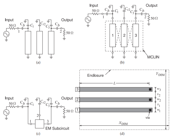
Figure \(\PageIndex{20}\): Physical layout of the combline bandpass filter designed in Section 3.4.1: (a) with discrete capacitors; (b) with a microstrip coupled transmission line element (MCLIN); (c) with an EM subcircuit block; and (d) the EM subcircuit block with layout to be simulated in an EM simulator. Details: \(6\:\mu\text{m}\) gold metalization, \(635\:\mu\text{m}\) thick alumina substrate with \(\varepsilon_{r} = 10, 400\:\mu\text{m}\times 400\:\mu\text{m}\) tantalum vias, and the EM enclosure has perfectly conducting walls with \(X_{\text{DIM}} = 22\text{ mm,} Y_{\text{DIM}} = 20\text{ mm,}\) and height \(= 5.635\text{ mm}\).
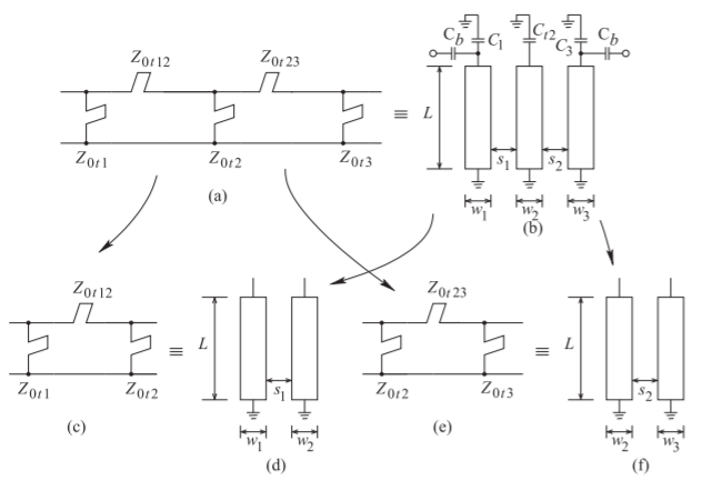
Figure \(\PageIndex{21}\): Physical design of the third-order combline bandpass filter. The double Pi network in (a) is partitioned into two Pi networks in (c) and (e). Similarly the three coupled microstrip lines in (b) are partitioned into two pairs of coupled lines in (d) and (f). Then physical design of the filter involves transforming the electrical design in (c) into the physical design in (d). Similarly the circuit in (e) is transformed into the layout in (f). With a shared central stub, the electrical circuit in (a) becomes the three coupled-line realization in (b).
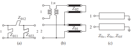
Figure \(\PageIndex{22}\): Equivalent circuits for a combline section (from Figure 3.2.13).
\[\label{eq:26}n=1+\frac{Z_{012}}{Z_{011}}=7.540,\quad Z_{02}=3342\:\Omega,\quad\text{and}\quad Z_{01}=69.17\:\Omega \]
The physical parameters of the coupled line pair in Figure \(\PageIndex{22}\)(c) are derived using the results in Section 5.9.6 of [29]. Thus
\[\label{eq:27}K=1/n=0.1326 \]
From Equations (5.197) and (5.198) of [29] two estimates of the system impedance, \(Z_{0S}\), are obtained:
\[\begin{align}\label{eq:28}Z_{0S, (3.54)}&=Z_{01}\sqrt{1-K^{2}}=68.56\:\Omega \\ \label{eq:29}Z_{0S, (3.55)}&=Z_{02}\frac{K^{2}}{\sqrt{1-K^{2}}}=59.30\:\Omega\end{align} \]
These two values of \(Z_{0S}\) are different and this is because the Pi arrangement of stubs is not symmetrical (i.e., in Figure \(\PageIndex{22}\)(a) \((Z_{011} = 67.7\:\Omega)\neq (Z_{022} = 80\:\Omega)\)).\(^{4}\) The assumption behind the development of Equations (3.2.3) and (3.2.4) are that the pair of coupled lines is symmetrical. The only reasonable choice is to use the geometric mean of the two values. So
\[\label{eq:30}Z_{0S}=Z_{0S,\text{ mean}}=\sqrt{Z_{0S, (3.54)}Z_{0S, (3.55)}}=63.77\:\Omega \]
Then, from Equation (5.202) of [29],
\[\label{eq:31}Z_{0o}=Z_{0S}\sqrt{\frac{n-1}{n+1}}=55.80\:\Omega,\quad Z_{0e}=\frac{Z_{0S}^{2}}{Z_{0o}}=72.87\:\Omega,\quad\text{and}\quad\frac{Z_{0e}}{Z_{0o}}=1.306 \]
The next step is to choose a substrate and realize the physical dimensions of the coupled lines. It is important that there be dimensional stability and that there be no multimoding. The best substrate for dimensional stability is a hard substrate like alumina, sapphire, or glass. Soft substrates like FR4 or teflon are too variable to be useful for filters. Alumina is particularly attractive as it is very hard and dimensions are reproducible. Alumina shrinks when it is processed but the amount of shrinkage is well controlled and reproducible. So once a design has been physically tuned, typically by drilling out part of the dielectric to change the effective permittivity, filters can be reliably reproduced and require only a small amount of adjustment. Alumina is polished to a well defined thickness and with a relative permittivity of around \(10\) a \(50-\Omega\) microstrip line has a width approximately equal to the thickness of the substrate. Having equal dimensions is a good thing to have for manufacturability. The thickness of the substrate must be decided on at this stage in design. A thicker substrate is less likely to crack during handling however a thicker substrate is more likely to support multimoding. Here a \((h =)\) \(635\:\mu\text{m}\)-thick alumina substrate with \(\varepsilon_{r} = 10\) is chosen and calculations (not shown here) indicate that there will not be multimoding at the filter’s operating frequencies.
Physical dimensions could be derived by iteratively solving for \(Z_{0e}\) and \(Z_{0o}\) using the formulas in Section 5.6 of [29]. As an approximation, here the physical dimensions are derived from Table 5-3 of [29]. Table 5-3 of [29] is for a system impedance, \(Z_{0S}\), of \(50\:\Omega\) and not the \(63.77\:\Omega\) found here. Thus there will be an error, but it can be expected that there will be error in any case and these can be resolved using optimization in a simulator. From Table 5-3 of [29], the initial physical dimensions of the pairs of lines are
\[\begin{align}\label{eq:32} u&= 0.93,\quad w = uh = 591\:\mu\text{m},\quad\text{thus with rounding}\quad w_{1} = w_{2} = w_{3} = 600\:\mu\text{m} \\ \label{eq:33} g&= 1.0,\quad s = gh = 635\:\mu\text{m},\quad\text{thus with rounding}\quad s_{1} = s_{2} = 650\:\mu\text{m}\end{align} \]
The rounding has been done as for EM simulation the lines will be laid out on a regular grid and a \(50\:\mu\text{m}\) grid is reasonable.
Scaling of Line Width
At this stage the error made with the characteristic impedance of the microstrip line should be considered. While any error can be corrected when optimizing the final design, making some correction at this stage will reduce the final adjustments needed. Three system impedances have been derived, \(Z_{0S,(3.54)} = 68.56\:\Omega,\: Z_{0S,(3.55)} = 59.30\:\Omega\), and the geometric mean \(Z_{0S\text{,mean}} = 63.77\:\Omega\). This divergence is one source of error. Another source of error is that a table for a \(50\:\Omega\) system impedance was used to determine the coupled-line parameters. Note that the electrical design is exact and the tuning of the physical design will attempt to match the response of the physical circuit to that of the electrical design. However some initial corrections will reduce the amount of tuning that needs to be done.
Scaling for the higher actual system impedance (\(63.77\:\Omega\) versus \(50\:\Omega\)) means using higher impedance microstrip lines (which will be narrower) and higher coupling impedance (requiring a greater separation of the lines). There are three possible characteristic impedance to scale to and a design decision needs to be made. Should the lines be scaled from \(50\:\Omega\) to \(54.2\:\Omega\), \(68.6\:\Omega\), or \(61.9\:\Omega\)? The most conservative approach is to scale from \(50\:\Omega\) to \(54.2\:\Omega\), a factor of \(1.08\). Here only adjustment of the line widths will be considered and two correction approaches will be described. The first is based on the rule of thumb described in Example 3.4 of [29] which indicated that the characteristic impedance of the microstrip lines is approximately proportional to \(1/\sqrt{w}\). So the line width should be reduced by a factor of \(1.082 = 1.17\) to shift the characteristic impedance. Thus the line width should be reduced from \(600\:\mu\text{m}\) to about \(600\:\mu\text{m}/1.17 = 512\:\mu\text{m}\) or \(500\:\mu\text{m}\) after rounding.
A second approach to correction is based on Table 3-3 of [29]. For \(\varepsilon = 10\) and using the more conservative system impedance (i.e. \(55.8\:\Omega\) which is closest to \(50\:\Omega\)), a better choice for \(u\) is to replace \(u = 0.93\) by \(u = 0.78\) and, after rounding, \(w_{1} = w_{2} = w_{3} = 500\:\mu\text{m}\). This cannot be expected to completely correct for the error, but it should be closer than the choice of \(600\:\mu\text{m}\).
Scaling the system impedance should also require that \(s\) be increased but there is not a simple guideline to follow and so this will be skipped. Another reason for needing to increase \(s\) is that there is more coupling in our coupled line system than that predicted by considering two pairs of coupled lines. For example, there is coupling from lines \(1\) directly to line \(3\). To reduce the coupling \(s\) will need to be increased, perhaps significantly. Another source
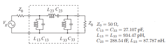
Figure \(\PageIndex{23}\): Lumped-element bandpass filter in a \(50\:\Omega\) system. (Derived by multiplying the impedances in Figure \(\PageIndex{6}\) by \(50\).)
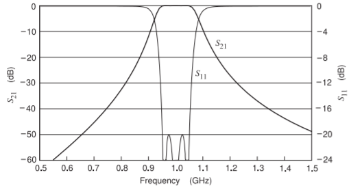
Figure \(\PageIndex{24}\): Return loss and insertion loss for the filter modeled using the lumped-element model.
of increased coupling is that the phase velocities of the even and odd modes differ. This tends to increase coupling. The adjustment of s is left to tuning of the physical design in an EM simulator.
Line Lengths
The stubs are one-eighth wavelength long at the center frequency of the filter. Thus the coupled lines are also one-eighth wavelength long. From Table 5-3 of [29], the effective relative permittivity of the even mode is \(\varepsilon_{ee} = 7.24\) and for the odd mode is \(\varepsilon_{eo} = 5.95\). These are quite different so the best that can be done is to use the geometric mean. Thus the effective relative permittivity is \(\varepsilon_{e} = \sqrt{\varepsilon_{ee}\varepsilon_{eo}} = 6.56\). Thus at \(1\text{ GHz}\) the line length \(L = \lambda_{8}/8 = \lambda_{0}/\sqrt{varepsilon_{e}} = (30\text{ cm})/(8\sqrt{6.56}) = 14.64\text{ mm}\) (\(14.65\text{ mm}\) with rounding). The use of a single effective permittivity in determining the lengths of the lines is perhaps the largest error and will result in the resonant frequency of each of the resonators, consisting of a capacitor (either \(C_{1},\: C_{t2},\) or \(C_{3}\)) and the \(\lambda/8\)-long line, being shifted from \(1\text{ GHz}\). The resonators can be re-centered by adjusting the capacitors. Adjusting the capacitance values also corrects for error in the widths of the lines since the main effect of an error in the width of a line is an error in its characteristic impedance and hence the input impedance of the resonator stub.
Microwave Circuit Simulation
Before simulating the combline filter the lumped-element bandpass filter will be considered to provide a benchmark. The \(50-\Omega\) lumped-element bandpass filter is shown in Figure \(\PageIndex{23}\). The responses of this filter is shown in Figures \(\PageIndex{24}\), \(\PageIndex{25}\), and \(\PageIndex{26}\). These responses provide a reference as the coupled-line
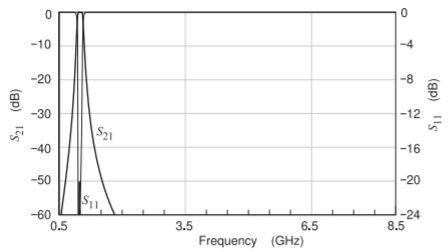
Figure \(\PageIndex{25}\): Wideband insertion loss and return loss for the filter modeled using the lumped-element model.
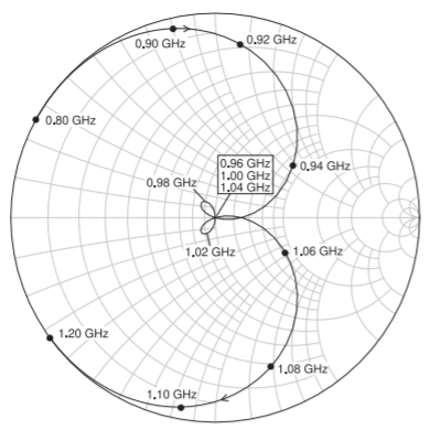
Figure \(\PageIndex{26}\): Plot of \(S_{11}\) on a Smith chart for the lumped-element bandpass filter. The zeros of the \(S_{11}\) response, and hence the poles of the \(S_{21}\) response, are at \(0.96,\: 1.00,\) and \(1.04\text{ GHz}\). The looping near the origin is characteristic of Chebyshev filters.
filter design is optimized.
Figure \(\PageIndex{20}\)(a) shows the combline filter to be modeled in a microwave circuit simulator. In a microwave simulator the filter can be modeled using a coupled microstrip element (known as the MCLIN element) or using EM simulation of an actual layout. The first set of results that will be presented uses the coupled microstrip element line model, the MCLIN element, and the filter model is as shown in Figure \(\PageIndex{20}\)(b). The results of the circuit simulation are shown in Figure \(\PageIndex{27}\). The curves (a) are responses for a gap of \(s = 650\:\mu\text{m}\). The passband is too wide and this is reduced by increasing \(s\) to \(1150\:\mu\text{m}\) yielding curves (b). The effect of loss is seen with \(S_{21}\) less than \(0\text{ dB}\) in the passband. The \(S_{21}\) response has a slight slope down in the passband and the \(S_{11}\) response does not show the three zeros seen in the lumped-element response, see Figure \(\PageIndex{24}\).
Plotting the \(S_{11}\) response of the MCLIN-based filter on a Smith chart, see Figure \(\PageIndex{28}\), provides more insight into what is happening. This should be contrasted to the \(S_{11}\) response of the lumped-element filter shown in Figure \(\PageIndex{26}\).
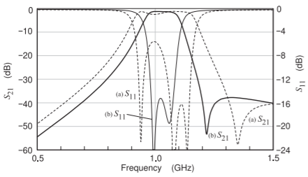
Figure \(\PageIndex{27}\): Insertion loss and return loss for the filter modeled using the MCLIN element with a line length of \(L = 14,650\:\mu\text{m}\) and line widths \(w_{1} = w_{2} = w_{3} = 500\:\mu\text{m}\). \(C_{1} = C_{3} = 1.6428\text{ pF}\), \(C_{t2} = 2.7076\text{ pF}\), and \(C_{b} = 1.2217\text{ pF}\). For curves (a) \(s_{1} = s_{2} = 650\:\mu\text{m}\) and for curves (b) \(s_{1} = s_{2} = 1150\:\mu\text{m}\).
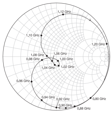
Figure \(\PageIndex{28}\): Plot of \(S_{11}\) on a Smith chart for filter modeled using the MCLIN element and gaps of \(s_{1} = s_{2} = 1150\:\mu\text{m}\) and a line length of \(L = 14,550\:\mu\text{m}\) and line widths \(w_{1} = w_{2} = w_{3} = 500\:\mu\text{m}\). \(C_{1} = C_{3} = 1.6428\text{ pF}\), \(C_{t2} = 2.7076\text{ pF}\), and \(C_{b} = 1.2217\text{ pF}\).
Recall that the lumped-element filter is the ideal electrical design. The looping of \(S_{11}\) at the origin in Figure \(\PageIndex{26}\) indicates that the ideal electrical response has three zeros as the locus of \(S_{11}\) passes through the origin three times. This behavior corresponds to the poles of the transmission response but these poles cannot be seen in the \(S_{21}\) response. Consequently in optimizing a filter the designer focuses on the \(S_{11}\) response.
Again consider the \(S_{11}\) responses of the two filters plotted on Smith charts (i.e. Figures \(\PageIndex{26}\) and \(\PageIndex{28}\)). The \(S_{11}\) response of the lumped-element filter has two small loops corresponding to peaks in the in-band \(|S_{11}|\) response seen in the rectangular plot of Figure \(\PageIndex{24}\). In contrast, the locus of \(S_{11}\) of the MCLIN-based filter does not go through the origin, see Figure \(\PageIndex{28}\), and there is one loop although the hint of a second loop is seen at \(1.06\text{ GHz}\). The performance is close to that required but optimization is necessary. In manually optimizing, also called tuning, the design of the MCLIN-based filter, both the rectangular and Smith chart plots should be overlaid with the lumped-element response. By adjusting \(C_{1},\: C_{t2}\), and \(C_{3}\) (by \(6\%,\: 16\%,\)
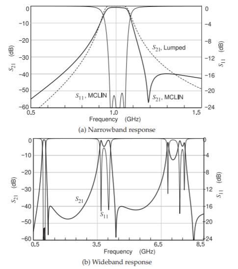
Figure \(\PageIndex{29}\): Insertion loss and return loss for the filter modeled using the MCLIN element and gaps of \(s_{1} = s_{2} = 1150\:\mu\text{m}\) and a line length of \(L = 14,550\:\mu\text{m}\) and line widths \(w_{1} = w_{2} = w_{3} = 500\:\mu\text{m}\). \(C_{1} = C_{3} = 1.9076\text{ pF},\: C_{t2} = 2.8748\text{ pF}\), and \(C_{b} = 1.2217\text{ pF}\).
and \(6\%\) respectively), the resonant frequencies of the resonators are centered at \(1\text{ GHz}\) and the filter response is also centered at \(1\text{ GHz}\)\(^{5}\). The result of this tuning is shown in Figures \(\PageIndex{29}\) and \(\PageIndex{30}\) indicating that the required performance has been obtained.
In Figure \(\PageIndex{29}\)(a) the MCLIN-based filter response is compared to the lumped-element response. The bandwidths of the MCLIN and lumped-element implementations are closely matched. The MCLIN implementation has the steep skirts resulting from the Chebyshev prototype. The Smith chart plot of \(S_{11}\) of the MCLIN-based filter is shown in Figure \(\PageIndex{30}\). The loops seen with the lumped-element response, in Figure \(\PageIndex{26}\), are seen but now there is an additional rotation with respect to frequency. This is because the MCLIN-based filter has additional transmission-line delays and hence frequency-dependent phase shift. Also the \(S_{11}\) response in Figure \(\PageIndex{30}\) is rotated by \(180^{\circ}\) from the \(S_{11}\) locus for the lumped-element filter (see Figure \(\PageIndex{26}\)). This is because of the additional inverter at the input of the distributed filter design.
Some gross features are seen in the combline response that are not seen in the ideal electrical response. Referring to Figure \(\PageIndex{29}\)(a), these include the additional zero seen in the \(S_{21}\) response at \(1.2\text{ GHz}\), the steeper skirt above
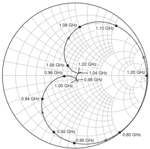
Figure \(\PageIndex{30}\): Plot of \(S_{11}\) on a Smith chart for filter modeled using the MCLIN element and gaps of \(s_{1} = s_{2} = 1150\:\mu\text{m}\) and a line length of \(L = 14,550\:\mu\text{m}\) and line widths \(w_{1} = w_{2} = w_{3} = 500\:\mu\text{m}\). \(C_{1} = C_{3} = 1.9076\text{ pF},\: C_{2} = 2.8748\text{ pF}\), and \(C_{b} = 1.2217\text{ pF}\).
the \(1\text{ GHz}\) passband, and the less-steep skirt below the passband. These are related. These features are common to PCL designs that use a combline. The origin of this behavior is the additional transmission path directly from the first line to the last line of the filter, the \(1-3\) coupling. During design the only transmission path considered was from line \(1\) to line \(2\), and then from line \(2\) to line \(3\), the \(1-2-3\) coupling. Apparently, at \(1.2\text{ GHz}\) the \(1-3\) and \(1-2-3\) signals have the same magnitude but opposite phase and so cancel producing the \(S_{21}\) zero. Above the passband the signals on the two paths destructively interfere causing the steeper skirt. Below the passband the \(1-3\) and \(1-2-3\) signals constructively interfere and reduce the steepness of the filter skirt. The additional zero can be exploited to significantly reduce the level of a particular signal such as a local oscillator or a signal in a neighboring communication band. If the reduced filter skirt below the passband is not acceptable, then another arrangement of coupled lines should be used.
Figure \(\PageIndex{29}\)(b) is a wideband response of the MCLIN-based filter and shows the spurious passbands that occur with most transmission-line based networks. In this case the properties of the lines are the same at \(\lambda/8,\: 5\lambda /8,\) and \(9\lambda /8\). So, by just considering the transmission lines alone it would be expected that there would be spurious passbands at \(5\text{ GHz}\) and \(9\text{ GHz}\). The spurious passbands are lower because the impedances of the capacitances reduce at the higher frequencies, resulting in the passbands at four times and seven times the center frequency of the filter. In practice, a simple lowpass filter eliminates the spurious passbands. Often parasitics in the system do this without specific circuitry. Also, appropriate choice of matching networks can provide adequate elimination of the spurious passbands.
Before finalizing the filter layout, a more accurate EM simulation is required instead of using the MCLIN element. The EM simulation captures more subtle effects than can be included in the MCLIN model. The layout of the parallel coupled lines is shown in Figure \(\PageIndex{20}\)(d) and the connection to incorporate these in a complete circuit simulation is shown in Figure \(\PageIndex{20}\)(c). The results of the EM-based simulation are shown in Figures \(\PageIndex{31}\) and \(\PageIndex{32}\). It can be seen that the bandwidth of the filter reduces. Additional optimization would result in the EM-based filter response more closely matching the ideal electrical response.
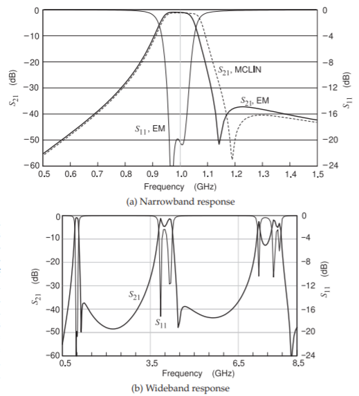
Figure \(\PageIndex{31}\): Return and insertion loss for the filter modeled using EM modeling and gaps of \(s_{1} = s_{2} = 1150\:\mu\text{m}\) and a line length of \(L = 14,550\:\mu\text{m}\) and line widths \(w_{1} = w_{2} = w_{3} = 500\:\mu\text{m}\). \(C_{1} = C_{3} = 1.9076\text{ pF},\: C_{t2} = 2.8748\text{ pF}\), and \(C_{b} = 1.2217\text{ pF}\).
3.4.3 Alternative Combline Filter Layouts
Up to a few gigahertz surface-mount capacitors can be used in the implementation of the capacitively-loaded stubs. Above that other arrangements should be considered. There are several layout variations for the combline filter. The main variations relate to replacing the lumped-element capacitors by gap capacitors and alternative realizations of the input and output inverters. Several variations are shown in Figure \(\PageIndex{33}\). The layout in Figure \(\PageIndex{33}\)(a) implements the capacitors using gap capacitors. At \(1\text{ GHz}\) it is difficult to realize the required capacitance using gap capacitors, then the interdigitated capacitors shown in Figure \(\PageIndex{33}\)(b) can be used to obtain higher capacitance values. Alternatively a coupled-line section can be used to implement the input and output inverters as shown in Figure \(\PageIndex{33}\)(c).
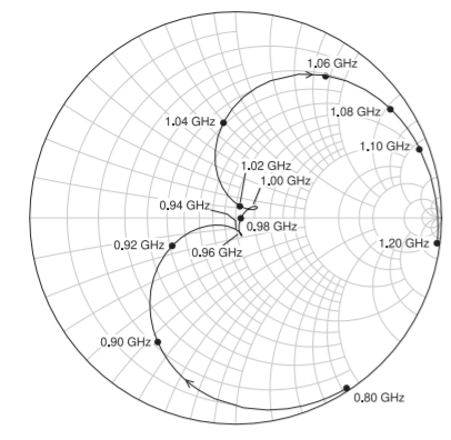
Figure \(\PageIndex{32}\): Plot of \(S_{11}\) on a Smith chart for filter modeled using EM modeling and gaps of \(s_{1} = s_{2} = 1150\:\mu\text{m}\), line length \(L = 14,550\:\mu\text{m}\), line widths \(w_{1} = w_{3} = w_{2} = 500\:\mu\text{m}\). \(C_{1} = C_{3} = 1.9076\text{ pF},\: C_{2} = 2.8748\text{ pF}\), and \(C_{b} = 1.2217\text{ pF}\).
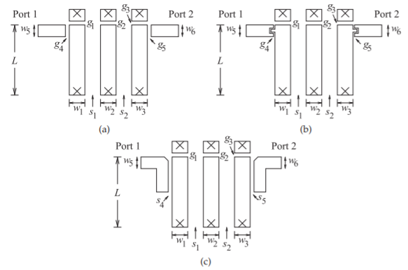
Figure \(\PageIndex{33}\): Physical layouts of the combline bandpass filter: (a) with gap capacitors having gaps of \(g_{1},\: g_{1},\ldots , g_{5}\),; (b) with interdigitated capacitors to obtain higher capacitance; and (c) with coupled lines (with separations \(s_{4}\) and \(s_{5}\)) realizing the input and output inverters.
Footnotes
[1] Of course there are resonant frequencies at every multiple of one-quarter wavelength. The first resonance occurs at \(f_{r}\), as then the input impedance of the short-circuited stub is an open circuit. The characteristic that establishes resonance is that the input is either an open- or short-circuit and energy is stored.
[2] What is reasonable for the width of a microstrip line is subjective and based on experience. With a substrate having \(\varepsilon_{r} = 10\), the width required for a characteristic impedance, \(Z_{0}\), of \(30–80\:\Omega\) is reasonable. A line with \(Z_{0} < 30\:\Omega\) will be very wide, use too much area, and potentially lead to multi-moding. A line with \(Z_{0} > 80\:\Omega\) will be narrow, close to the maximum \(Z_{0}\) that can be realized in a technology, have manufacturing tolerance issues, and have large radiation. The range can be extended to \(20–100\:\Omega\) but typically with degraded performance. Also see Example 3.4 of [29] for a microstrip design guideline.
[3] Note that the precision has been reduced. It was necessary to retain high precision during the electrical synthesis but the physical dimensions do not need the same precision.
[4] Thus error is being introduced at this step. In reality the final manufactured filter will need to be tuned anyway as the filter will require tolerances of about \(0.1\%\) or better and the best manufactured dimensional tolerance is usually about \(1\%\). Also material parameters are usually not known to better than \(1\%\). So this is an error that must be accepted.
[5] Approximately, the resonant frequency of a resonator is inversely proportional to \(\sqrt{C}\). So increasing the capacitances will reduce the center frequency of the filter.