
5.2: Diodes
- Page ID
- 46127

Diodes are two-terminal devices that have nonlinear current-voltage characteristics. The most common diodes used in microwave engineering are listed in Table 5.1.1 along with their standard symbols. Ideally a rectifier allows current to flow in one direction and not in the other. A general diode, usually a junction diode or a Schottky diode, is one type of rectifier, but rectifiers are more general, and, for example, they can be realized using vacuum devices.
Junction and Schottky Diodes
Junction diodes are two-terminal devices that derive their characteristics from the barrier effect that occurs at the junction of two different types of semiconductor (one with excess free holes and one with excess free electrons), or at the interface of a metal and a semiconductor. The result is an asymmetric current-voltage characteristic, as shown in Figure \(\PageIndex{1}\)(a). This is not an ideal rectifier characteristic, as it requires a threshold voltage to be reached before there is appreciable current flow. Semiconductor-based diode
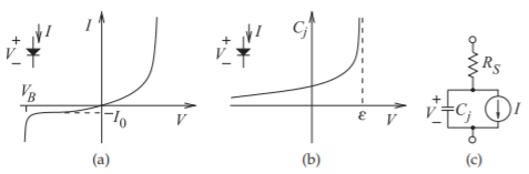
Figure \(\PageIndex{1}\): Characteristics of a pn junction diode or a Schottky diode: (a) current-voltage characteristic; (b) capacitance-voltage characteristic; and (c) diode model.
characteristics are described by [4, 5, 6]
\[\label{eq:1}I=I_{0}\left[\text{exp}\left(\frac{qV}{nkT}\right)-1\right] \]
where \(V\) is the voltage across the junction, \(q(= −e)\) is the absolute value of the charge of an electron, \(k\) is the Boltzmann constant \((1.37\cdot 10^{−23}\text{ J/K})\), and \(T\) is the absolute temperature (in kelvin). \(I_{0}\) is the reverse saturation current and is small, with values ranging from \(1\text{ pA}\) to \(1\text{ nA}\). The quantity \(n\) is the diode ideality factor, with \(n = 2\) for graded-junction pn junction diodes and \(n = 1.0\) for step-junction diodes where the interface between p-type and ntype semiconductor materials is abrupt. The abrupt junction is most closely realized by a Schottky diode, where a metal forms one side of the interface (typically) replacing the p-type semiconductor. Carriers recombine quickly in the metal, much faster than they would in a semiconductor. Hence a Schottky diode operates at higher frequencies than does a pn junction diode. A unity ideality factor, \(n\), of \(1\) is the best that can be achieved, resulting in the strongest nonlinearity. When the applied voltage is sufficiently positive to cause a large current to flow, the diode is said to be forward biased. When the voltage is negative, the current flow is negligible and the diode is said to be reverse biased. At sufficiently large reverse bias, electrons are ripped from the valence bands of the semiconductor atoms and the current rapidly increases in a process called impact ionization or avalanche. The voltage at which this occurs is called the reverse breakdown voltage.
In a semiconductor diode, charge is separated over distance and so a diode has appreciable capacitance, called the junction capacitance, mathematically modeled as
\[\label{eq:2}C_{j}(V)=\frac{C_{j0}}{(1-(V/\phi))^{\gamma}} \]
where \(\phi\) is the built-in potential difference across the diode. This capacitance profile is shown in Figure \(\PageIndex{1}\)(b). The built-in potential is typically \(0.6\text{ V}\) for silicon diodes and \(0.75\text{ V}\) for GaAs diodes. The doping profile can be adjusted so that \(\gamma\) can be less than the ideal \(\frac{1}{2}\) of an abrupt junction diode.
Current must flow through bulk semiconductor before reaching the active region of the semiconductor diode, and so there will be a resistive voltage drop. Combining effects leads to the equivalent circuit of a pn junction or Schottky diode shown in Figure \(\PageIndex{1}\)(c).
Varactor Diode
A varactor diode is a pn junction diode operated in reverse bias and optimized for good performance as a tunable capacitor. Ideally it has low reverse saturation current, high reverse breakdown voltage, and a specific capacitance profile designed for a particular application.
A common application of a varactor diode is as the tunable element in a voltage-controlled oscillator (VCO) where the varactor, with voltage-dependent capacitance, \(C\), is part of a resonant circuit (often called a tank circuit) with a lumped inductor, \(L\). The resonant frequency of the tank circuit is proportional to \(1/\sqrt{LC}\), so by applying a voltage to a varactor diode, \(C\) changes, the resonant frequency of the tank circuit is tuned, and the oscillation frequency is changed. The capacitance versus voltage is described by Equation \(\eqref{eq:2}\) and voltage dependence is shown in Figure \(\PageIndex{1}\)(b).
PIN Diode
A PIN diode is a variation on a pn junction diode with a region of intrinsic semiconductor (the I in PIN) between the p-type and n-type semiconductor regions. The properties of the PIN diode depend on whether there are carriers in the intrinsic region. The PIN diode has the current-voltage characteristics of a pn junction diode at low frequencies; however, at high frequencies it looks like a linear resistor, as carriers in the intrinsic region move slowly. When a forward DC voltage is applied to the PIN diode, the intrinsic region floods with carriers, and at microwave frequencies the PIN diode is then modeled as a low-value resistor. At high frequencies there is not enough time to remove the carriers in the intrinsic region, so even if the total voltage (DC plus RF) across the PIN diode is negative, there are carriers in the intrinsic region throughout the RF cycle. If the DC voltage is negative, carriers are removed from the intrinsic region and the diode looks like a large-value resistor at RF. The PIN diode can be used as a microwave switch controlled by a DC voltage.
Zener Diode
Zener diodes are pn junction or Schottky diodes that have been specially designed to have sharp reverse breakdown characteristics [5]. They can be used to establish a voltage reference or, used as a limiter diode, to provide protection of more sensitive circuitry. As a limiter, they are found in communication devices in a back-to-back configuration to limit the voltages that can be applied to sensitive RF circuitry.
LED Diode
In semiconductor diodes, the recombination of holes and electrons can result in photons being generated. This effect is enhanced to form light-emitting diodes (LEDs) [4, 5, 7, 8].