
5.3: Case Study- Tunable Resonator with Varactor Diode Stack
- Page ID
- 46128

Varactors provide a tunable capacitance with the bias voltage across the varactor, a reverse biased diode, changing the capacitance of the diode. The applied bias voltage also changes the series resistance of the diode, see Figure 5.2.1. The characteristics of a microwave varactor are shown in Figure \(\PageIndex{1}\). At a reverse bias voltage \(V_{R} = 1\text{ V}\) the junction capacitance \(C_{j} = 7\text{ pF}\) and the series resistance is \(1.8\:\Omega\). At \(5\text{ GHz}\) the diode impedance \(Z_{D}(1\text{ V})=1.8 −\jmath 4.54\:\Omega\) and its \(Q(1\text{ V})=2.5\). At a reverse bias voltage \(V_{R} = 10\text{ V}\), the junction capacitance \(iC_{j} = 1\text{ pF}\), and the series resistance is \(0.4\:\Omega\). At \(5\text{ GHz}\) the diode impedance \(Z_{D}(1\text{ V})=0.4 −\jmath 31.8\:\Omega\) and its \(Q(1\text{ V}) = 80\).
Generally a design proceeds based on a chosen system impedance which is often \(50\:\Omega\) so that the design space includes realizable impedances above and below a system impedance. One way of effectively increasing the impedance of a varactor diode is to stack diodes. This is shown in Figure \(\PageIndex{2}\) where four
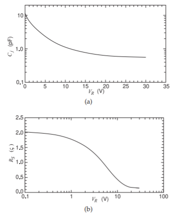
Figure \(\PageIndex{1}\): Characteristics of a varactor diode (Toshiba model JDV2S71E1, a silicon epitaxial planar diode) as a function of reverse bias voltage \(V_{R}\): (a) capacitance \(C_{j}\) ; and (b) series resistance \(R_{S}\).
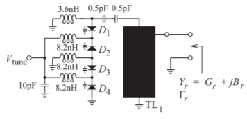
Figure \(\PageIndex{2}\): A stub-loaded diode stack resonator designed to produce a variable capacitance in the \(4–6\text{ GHz}\) range. The element labeled TL1 is a low impedance microstrip line. The choke inductor, \(L_{\text{CHOKE}} = 8.2\text{ nH}\), presents an RF open circuit and is part of the bias circuit. Each varactor diode \((D_{1}–D_{4})\) is model JDS2S71E.
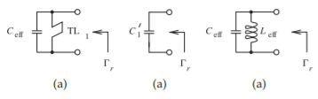
Figure \(\PageIndex{3}\): Equivalent circuits of the stubloaded diode stack resonator of Figure \(\PageIndex{2}\).
varactor diodes \(D_{1},\ldots ,D_{4}\) are shown together with the biasing arrangement so that the each of the diodes can be adjusted by the single tuning voltage \(V_{\text{tune}}\) applied through the \(3.6\text{ nH}\) and \(8.2\text{ nH}\) choke inductors. The choke inductors provide a DC short and an RF open (actually an impedance magnitude of \(258\:\Omega\) for the \(8.2\text{ nH}\) inductor at \(5\text{ GHz}\)). Figure \(\PageIndex{2}\) is the schematic of a tunable resonator, used between \(4\) and \(5.3\text{ GHz}\) to tune an oscillator, see [9] and Section 5.6 of [10].
The two \(0.5\text{ pF}\) capacitors in Figure \(\PageIndex{2}\) scale the capacitance of the diode stack and increase the effective \(Q\) of the variable capacitance. The shorted transmission line presents an inductance impedance in shunt with the augmented diode stack. A lumped inductor is not used here as it would have too high a loss. The equivalent circuit of the resonator is shown in Figure \(\PageIndex{3}\). The resonator network is designed to be resonant at a frequency above the operating frequency. At the oscillation frequency the resonator network must present an inductance to resonate with the capacitance of the active device in an oscillator. In addition, for oscillator stability, the effective inductance must have a particular derivative of admittance with respect to frequency.
The two \(0.5\text{ pF}\) capacitors between TL1 and the varactor stack combine to provide an effective capacitance of \(0.25\text{ pF}\) which has an impedance of \(127\:\Omega\) at \(5\text{ GHz}\). So it is not a DC blocking capacitor which would have a very low impedance at RF, but it does block DC so that \(V_{\text{tune}}\) is not shorted to ground through the transmission line. The RF function of the two series \(0.5\text{ pF}\) capacitors is to reduce the value of the variable capacitance, increase the operating reactance, and increase the \(Q\) of the effective capacitance. Each varactor diode has a \(0\text{ V}\) capacitance of \(11\text{ pF}\) and a capacitance at \(9\text{ V}\) of \(2.15\text{ pF}\). With the four varactors in series this becomes \(2.75\text{ pF}\) total capacitance at \(0\text{ V}\) and \(0.54\text{ pF}\) at \(9\text{ V}\). The \(0.25\text{ pF}\) capacitance in series reduces this to \(0.229\text{ pF}\) at \(0\text{ V}\) tuning voltage and \(0.171\text{ pF}\) at \(9\text{ V}\) tuning voltage for a capacitance tuning ratio of \(0.229\text{ pF}/0.171\text{ pF} = 1.34\). The capacitance tuning range has been reduced from the original ratio of \(2.75\text{ pF}/ 0.54\text{ pf} = 5.05\). The tuning range of the resonant frequency of a parallel \(LC\) resonator is the square root of this, i.e. \(1.16\) (which comes from the resonant frequency being \(1/\sqrt{LC}\)). If this is not enough the two \(0.5\text{ pF}\) capacitors can be changed to achieve the required overall capacitance tuning ratio.
The \(10\text{ pF}\) capacitor between the \(V_{\text{tune}}\) terminal and ground is there to ensure an RF short circuit. The magnitude if the impedance of this capacitor at \(5\text{ GHz}\) is \(3.2\:\Omega\), a factor of ten away from the \(50\:\Omega\) system impedance. While at RF the terminal at \(V_{\text{tune}}\) is ideally a short circuit to ground, there will always be some wiring inductance.
The characteristics of the resonator can be understood by looking at the plot of the simulated resonator reflection coefficient, \(\Gamma_{\Gamma}\), on a Smith chart, see Figure \(\PageIndex{4}\). \(\Gamma_{\Gamma}\) is shown for two tuning voltages as well as the device locus of the inverse of the input reflection coefficient of a transistor circuit
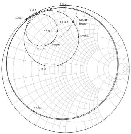
Figure \(\PageIndex{4}\): Simulated reflection coefficient of the resonator, \(\Gamma_{\Gamma}\) on a \(50\:\Omega\) Smith chart for two tuning voltages (\(1\text{ V}\) and \(3\text{ V}\)). The drive locus shown is the inverse of the input reflection coefficient of an active network that would be connected at the same port as for \(\Gamma_{\Gamma}\). The intersection of \(\Gamma_{\Gamma}\) and the drive locus determines the operating frequency.
connected to the resonator. The combination of the resonator and the active device forms an oscillator. The intersection of the active device and resonator loci selects the oscillation frequency of the oscillator. The oscillator presents a capacitance to the resonator and so the resonator must present an inductance to the active device. The frequency of the oscillator is varied by changing \(\Gamma_{\Gamma}\) of the resonator
A photograph of the resonator is shown in Figure \(\PageIndex{5}\). The measured \(\Gamma_{\Gamma}\) is shown in Figure \(\PageIndex{6}\) and this corresponds to the simulated plot in Figure \(\PageIndex{4}\). The two plots are roughly in agreement but there is a discrepancy because it is very hard to do these measurements at \(5\text{ GHz}\), and the models of the device components are not exact. However the main reason for the discrepancy is that this is a measurement of a resonant circuit and small discontinuities can have a dramatic effect. What is presented here is typical of microwave circuit design and why tremendous intuition is required to design at microwave frequencies and to interpret measurements.
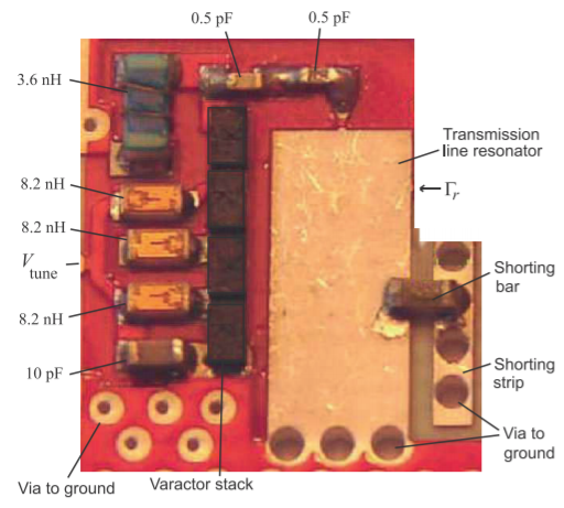
Figure \(\PageIndex{5}\): Photograph of the microstrip resonator network with surface mount components. The shorting bar is a \(0\:\Omega\) surface mount resistor and is used to adjust the effective length of the transmission line resonator, \(\text{TL}_{1}\).
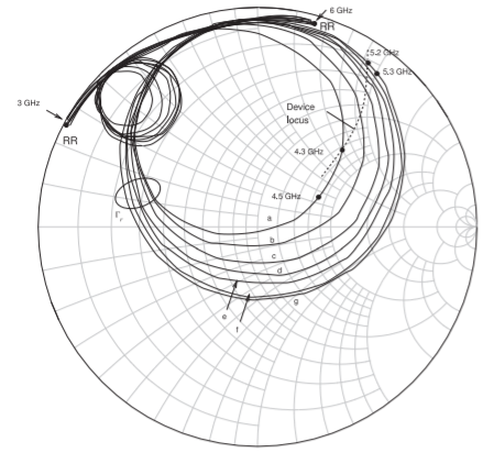
Figure \(\PageIndex{6}\): Measured reflection coefficient of the resonator network, \(\Gamma_{\Gamma}\). Curve \(a\), is the characteristic of the resonator network for a tuning voltage, \(V_{\text{tune}}\), of \(0\text{ V}\). Curve \(g\) is for \(V_{\text{tune}} = 9\text{ V}\). \(V_{\text{tune}}\) is equally spaced for Curves \(a– g\). The inverse of the reflection coefficient of an active device connected at the \(\Gamma_{\Gamma}\) point is shown and indicates that the active device presents a negative conductance. The intersection of the device locus and \(\Gamma_{\Gamma}\) determines the oscillation frequency of an oscillator. Thus adjusting \(V_{\text{tune}}\) changes the oscillation frequency.