
7.1: Introduction
- Page ID
- 46149
Design of a receiver or transmitter circuit requires the design of a cascade of modules that achieves optimum dynamic range while managing DC power consumption. As an example the frequency conversion stage of a receiver is shown in Figure \(\PageIndex{1}\). The microstrip filters and transmission lines are fabricated on alumina substrates. The semiconductor dies and the chip decoupling capacitors as well as the alumina modules are epoxied to a mat that was screen-printed on a brass housing. The mat provides a stress-relieving (allowing for differences in thermal coefficients of expansion) and conducting interface between the alumina and semiconductor substrates and the brass housing. The modules and dies are interconnected by bond wires arranged as two or more bond wires in parallel to reduce inductance. The bond wires attach to the pads on the decoupling capacitors. These modules, with the exception of filters, are described in this chapter.
The chapter begins with investigation of a cascade of modules given the distortion characteristics of the individual modules. Coupled with an earlier treatment of noise of a cascaded system this defines dynamic range. A microwave systems comprising a cascade of mostly two-port modules and must be designed to simultaneously minimize noise, distortion, DC power consumption, spurious emissions, and maximize dynamic range. There is necessarily a trade-off of these performance parameters and this trade-off is at the heart of system design. What makes this particularly challenging is that the two-port networks are designed separately and there
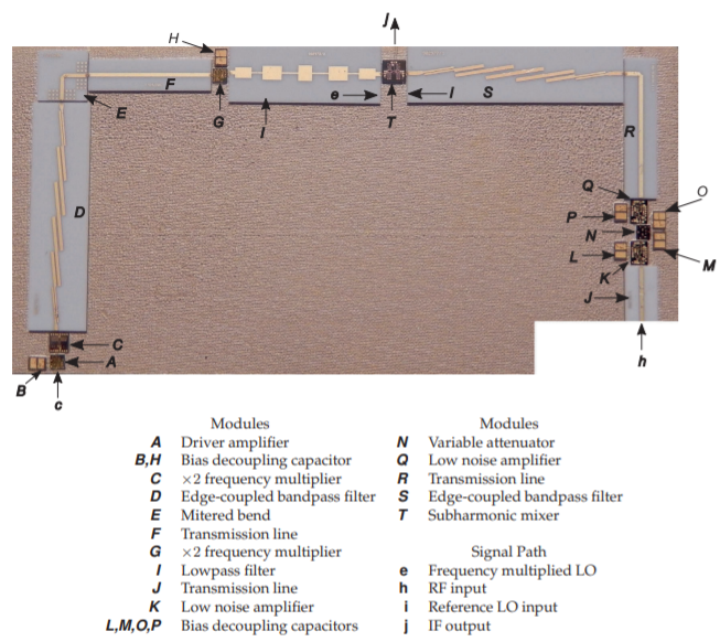
Figure \(\PageIndex{1}\): The frequency conversion portion of the \(15\text{ GHz}\) receiver shown in Figure 7.6.1. The RF input at \(\mathbf{h}\) is centered at \(15\text{ GHz}\) and is amplified and filtered before being presented to athe subharmonic mixer at \(\mathbf{T}\). The reference LO at \(\mathbf{c}\) is tunable from \(1601\) to \(1742\text{ MHz}\) and is frequency multiplied twice, at \(\mathbf{C}\) and \(\mathbf{G}\), and then presented as the LO to the harmonic mixer at at \(\mathbf{T}\). The LO ranges from \(6403\) to \(6968\text{ MHz}\). The IF output at \(\mathbf{j}\) ranges from \(465\) to \(1595\text{ MHz}\).
is incomplete characterization of performance. Indeed the only accurate way of determining overall system performance would be to have the circuit-level schematics of each module and then perform a whole system time-domain circuit-level simulation using the actual modulated signals. Even if all the details were available the simulation time would be prohibitive and a time-domain simulation is unlikely to have the necessary fidelity. This is true even if a large part of a system is implemented on the same chip. Thus system design must use a methodical process using incomplete module-level parameters such as the \(1\text{ dB}\) gain compression, noise figure, and third-order intercept characterizations. System design is often conservative designing for worst case. Sometimes this is too conservative and allowances must be made.
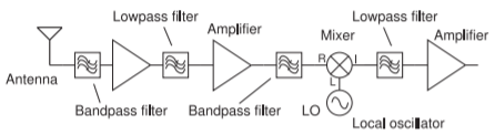
Figure \(\PageIndex{2}\): Receiver as a cascade of modules.
Testing and adjustment of fabricated prototypes is essential.
This section describes two approaches to cascaded module design; the budget method and the contribution method. In the budget method gain and noise performance metrics are initially assigned to each stage in a cascade and then these are adjusted in a system simulator to iterate towards an optimum solution. In the contribution method the focus is on dynamic range and each critical module is assigned the same dynamic range and from this an initial assignment of noise figure, gain, and required linearity is made for each module. The optimization of system performance proceeds as with the budget method. Generally this optimization must be performed manually using experience as often it is difficult to quantify what an optimum is. Also some design decisions require the acquisition of higher cost modules and if a module is low cost then it makes sense to assign high dynamic range to such a module to reduce the requirements on other higher cost modules. Perhaps a module must be redesigned or designed in-house instead of being externally sourced. These are not simple decisions. In the end, the system with cascaded modules must be cost and performance competitive, and reducing time to market is a competitive advantage.