
3.4: Receiver and Transmitter Architectures
- Page ID
- 41190

The essential function of a radio transmitter architecture is taking low-frequency information, the baseband signal, and transferring that information to much higher frequencies by superimposing the baseband signal on a high-frequency carrier, i.e a sinewave. This could be done by slowly varying the amplitude, frequency, and/or phase of the carrier in what is called modulating the carrier to produce a modulated carrier (signal). A caveat here is that there are other less common ways of transferring the baseband information such as rapidly changing the frequency of the carrier at a faster rate than the maximum frequency of the baseband signal in a scheme called frequency hoping. Frequency hoping is particularly useful when operating in hostile situations, such as military communications, when the interference environment cannot be controlled. In reality there is a very large number of ways of producing a radio signal that carries the baseband information. The central theme of this book is to focusing on modulation schemes that slowly modulate characteristics of a carrier signal and other schemes are introduced as an exception. This section describes early architectural developments that led to the development of the regulations that still guide modern architectures; concepts that efficiently pack as much information as possible into a fixed RF bandwidth.
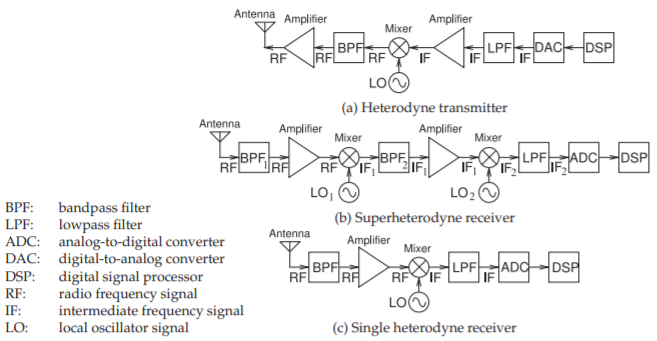
Figure \(\PageIndex{1}\): RF front ends: (a) a one-stage transmitter; (b) a receiver with two mixing (or heterodyning) stages; and (c) a receiver with one heterodyne stage.
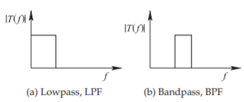
Figure \(\PageIndex{2}\): Ideal filter responses where \(T(f)\) is the transmission response as a function of frequency \(f\).
3.4.1 Radio as a Cascade of Two-Ports
The front end of an RF communication receiver or transmitter combines a number of subsystems in cascade. The design of the RF front end requires trade-offs of noise generated by the circuit, of frequency selectivity, and of power efficiency, which translates into battery life for a communication handset. There are only a few receiver and transmitter architectures that achieve the optimum trade-offs. The essentials of these architectures are shown in Figure \(\PageIndex{1}\). These architectures achieve frequency selectivity using bandpass filters (BPFs) and lowpass filters (LPFs) which ideally have the responses shown in Figure \(\PageIndex{2}\). The corner frequencies of these filters and, in the case of the BPFs, their center frequencies, are adjusted to minimize interfering signals and noise that passes through the system. The three architectures shown in Figure \(\PageIndex{1}\) have antennas that interface between circuits and the outside world. Antennas generally have a broad bandwidth, much greater than the bandwidth of an individual communication channel.
3.4.2 Heterodyne Transmitter and Receiver
First consider the transmitter architecture shown in Figure \(\PageIndex{1}\)(a). In a transmitter, a low-frequency information-bearing signal is translated to a frequency that can be more easily radiated. The information is contained in the baseband signal, which in many modern systems is generated as a digital signal within the digital signal processor (DSP). Then the digital-to-analog converter, (DAC), converts the digital baseband to an analog signal called the analog baseband, identified in Figure \(\PageIndex{1}\)(a) as the intermediate frequency (IF) signal at the output of the DAC. Older systems generate the IF signal using analog hardware as this reduces the power consumed by the digital electronics. The IF then passes through a lowpass filter (LPF) to remove the harmonics resulting from the DAC process, and the signal is then amplified before being applied to the mixer. There are several types of mixers, but the central concept is multiplying the IF signal by a much larger local oscillator (LO) signal at frequency \(f_{\text{LO}}\). The LO will be a single cosinusoid and if its amplitude is \(A_{\text{LO}}\), then the LO signal is \(x_{\text{LO}} = A_{\text{LO}}\cos(2πf_{\text{LO}})\). While the IF signal will have a finite bandwidth, the operation of the mixer can be illustrated by considering that the IF is a single cosinusoid with amplitude \(A_{\text{IF}}\) and frequency \(f_{\text{IF}}\), that is the RF signal is \(x_{\text{IF}} = A_{\text{IF}}\cos(2πf_{\text{IF}})\). Then the output of the mixer is
\[\begin{align}x_{\text{RF}}&=x_{\text{IF}}\times x_{\text{LO}}=A_{\text{IF}}A_{\text{LO}}\cos (2\pi f_{\text{IF}})\cos (2\pi f_{\text{LO}})\nonumber \\ \label{eq:1}&=\frac{1}{2}A_{\text{RF}}A_{\text{LO}}\{\cos [2\pi (f_{\text{LO}}-f_{\text{IF}})]+\cos [2\pi (f_{\text{LO}}+f_{\text{IF}})]\}\end{align} \]
In Equation \(\eqref{eq:1}\) a trigonometric expansion has been used. The LO is chosen so that its frequency is close to that of the desired RF so that multiplication by the mixer results in an output that has one component at \(f_{\text{RF}\Delta} = f_{\text{LO}}−f_{\text{IF}}\) and one at \(f_{\text{RF}\sum} = f_{\text{LO}} + f_{\text{IF}}\). One of these is selected by the BPF, is further amplified, and then delivered to the antenna and radiated.
3.4.3 Superheterodyne Receiver Architecture
The first receiver architecture to be considered is the superheterodyne (or superhet) receiver architecture shown in Figure \(\PageIndex{1}\)(b). Heterodyning refers to the use of a mixer and a superheterodyne circuit has two mixers. The antenna collects information from the environment at RF, and immediately this is bandpass filtered (by the \(\text{BPF}_{1}\) block) to eliminate most of the interfering signals and noise. Thus the first BPF reduces the range of voltages presented to the first amplifier and so reduces the chance that the amplifier will distort the desired signal.
The RF at the output of the leftmost bandpass filter, BPF1, still has a spectrum that is much broader than that of the desired communication signal. For example, in 3G radio the communication channel is \(5\text{ MHz}\) wide but the first BPF could be \(50\text{ MHz}\) wide and the RF could be \(1\text{ GHz}\) or \(2\text{ GHz}\). So it is still necessary to use additional frequency selectivity to isolate the single required channel. The optimum choice at this stage is to follow the first BPF with an amplifier to boost the level of the signal. This also boosts the level of the noise that was captured by the antenna along with the signal, but it means that the noise added by the circuitry after the first amplifier has much less importance. The next block in the receiver is the mixer that shifts the information down in frequency to the first intermediate frequency, \(\text{IF}_{1}\). The local oscillator, \(\text{LO}_{1}\), is chosen so that its frequency is close to that of the RF so that multiplication by the mixer results in a low frequency at the output (i.e., at \(f_{\text{IF1}} = f_{\text{LO}} − f_{\text{RF}}\)), and one at a frequency nearly twice that of the LO (i.e., at the sum frequency, \(f_{\sum} = f_{\text{LO}} +f_{\text{RF}}\)). The center frequency and
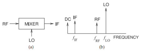
Figure \(\PageIndex{3}\): Simple mixer circuit: (a) block diagram; and (b) spectrum.
bandwidth of the second bandpass filter, \(\text{BPF}_{2}\), is chosen so that only the signals around \(f_{\text{IF1}}\) pass through. Thus the main function of the first mixer stage and \(\text{BPF}_{2}\) in the superheterodyne receiver is to convert the information at the RF down to a lower frequency, here at \(\text{IF}_{1}\). The operation of the mixer is shown in Figure \(\PageIndex{3}\).
In the superheterodyne receiver architecture the output of the first mixer, \(f_{\text{IF1}}\), is still at too high a frequency for the signal to be directly converted into digital form where it can be processed. So it is natural to ask why the frequency translation was not all the way down to baseband. The main reason for this is that there is substantial noise on an LO at frequencies very close to the oscillation frequency, \(f_{\text{LO1}}\). This noise drops off quickly away from the oscillation frequency and its level at frequency \(f\) is proportional to \((|f − f_{\text{LO1}}|)^{n},\: n = 1, 2,\ldots\). This noise will appear at the output of the mixer and will be substantial if the RF and LO are very close in frequency. So the optimum trade-off is to shift the frequency of the information-bearing signal in two stages. Following further amplification, the second stage of mixing converts the information-bearing component of the signal centered at the first intermediate frequency, \(\text{IF}_{1}\), to the second intermediate frequency, \(\text{IF}_{2}\), which is usually at the baseband frequency or slightly above it. The baseband signal is now analog and this is converted to digital form by the ADC, and then the signal, now the digital baseband signal, can be digitally processed by the DSP.
Since the second mixer operates at much lower frequencies than the first mixer, the phase noise on \(\text{LO}_{2}\) does not overlap the signal at \(\text{IF}_{2}\). The reason why this architecture is called a superheterodyne receiver architecture is because when this architecture was first used, \(\text{IF}_{2}\) was an audio signal and \(\text{IF}_{1}\) was above the audible range and so was a supersonic signal. Thus the super in superheterodyne initially referred to the supersonic IF.
3.4.4 Single Heterodyne Receiver
The second receiver architecture shown in Figure \(\PageIndex{1}\)(c) has a single heterodyne or mixing stage. If the LO has very low noise the IF will be at a lower frequency than in the superheterodyne architecture shown in Figure \(\PageIndex{1}\)(b). A high-performance ADC is then required to convert the signal to digital form and deliver it to the DSP unit. Substantial digital processing power is required to translate the signal to a digital baseband signal. Alternatively a high-performance subsampling ADC could be used that in effect performs mixing during conversion. The advantage of this architecture is a simplified RF section and is of particular advantage when multiple RF communication standards are supported as the DSP and ADC can be common while the analog RF hardware for each band is considerably simplified.
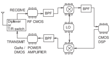
Figure \(\PageIndex{4}\): RF front end organized as multiple chips. This corresponds to a combination of the receive architecture shown in Figure \(\PageIndex{1}\)(c) and the transmitter architecture shown in Figure \(\PageIndex{1}\)(a).
3.4.5 Transceiver
The major transistor- or diode-based active elements in the RF front end of both the transmitter and receiver are the amplifiers, mixers, and oscillators. These subsystems have much in common, using nonlinear devices to convert power at DC to power at RF. In the case of mixers, power at the LO is also converted to power at RF. The front end of a typical cellphone is shown in Figure \(\PageIndex{4}\). The components here are generally implemented in a module and use different technologies for the various elements, optimizing cost and performance.
Return now to the mixer-based transceiver (for transmitter and receiver) architecture shown in Figure \(\PageIndex{4}\). Here, a single antenna is used, and either a diplexer\(^{1}\) (a combined lowpass and highpass filter) or a switch is used to separate the (frequency-spaced) transmit and receive paths. If the system protocol requires transmit and receive operations at the same time, a diplexer is required to separate the transmit and receive paths. This filter tends to be large, lossy, or costly (depending on the technology used). Consequently a transistor switch is preferred if the transmit and receive signals operate in different time slots. In the receive path the low-level received signal is amplified and the initial amplifier needs to have very good noise performance. Once the signal is larger the noise performance of the amplifiers is less critical. The initial amplifier is called a low-noise amplifier (LNA). The amplified receive signal is then bandpass filtered and frequency down-converted by a mixer to IF that can be sampled by an ADC to produce a digital signal that is further processed by DSP. Variants of this architecture include one that has two mixing stages (as in the superheterodyne receiver shown in Figure \(\PageIndex{1}\)(b)), and another with no mixing that relies instead on direct conversion of the receive signal using, as one possibility, a subsampling ADC. In the transmit path, the architecture is reversed, with a DAC driven by the DSP chip that produces an information-bearing signal at the IF which is then frequency up-converted by a mixer, bandpass filtered, and amplified by what is called a power amplifier to generate the tens to hundreds of milliwatts required.
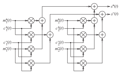
Figure \(\PageIndex{5}\): Differential implementation of a Hartley SSB-SC modulator: \(s^{+}(t),\: s^{−}(t)\) are the positive and negative components of the differential modulated signal \(s(t); (c_{1}^{+}(t),\: c_{1}^{−}(t))\) is the differential carrier; \((m_{1}^{+}(t),\: m_{1}^{−}(t))\) is the differential quadrature-modulated IF carrier; \((c_{2}^{+}(t),\: c_{2}^{−}(t))\) is the differential carrier shifted \(90^{\circ}\); and \(m_{2}^{+}(t)\) and \(m_{2}^{−}(t)\) are the \(90^{\circ}\) phase-shifted versions of \(m_{1}^{+}(t)\) and \(m_{1}^{−}(t)\), respectively.
3.4.6 Hartley Modulator
The Hartley modulator [1, 2], shown in Figure 3.1.1, results in SSB single-sideband (SSB) modulation or more precisely SSB suppressed-carrier (SSB-SC) modulation. This is one of the great inventions and variants of this circuit are used in all modern radios. In the Hartley modulator the modulating signal \(m(t)\) and the carrier are multiplied together in a mixer and then also \(90^{\circ}\) phase-shifted versions are also mixed before being added together. The signal flow is as follows beginning with \(m(t) = \cos(\omega_{m1}t),\: p(t) = \cos(\omega_{m1}t − π/2) = \sin(\omega_{m1}t)\) and carrier signal \(c_{1}(t) = \cos(\omega_{c}t)\):
\[\begin{align}a_{1}(t)&=\cos (\omega_{m1}t)\cos(\omega_{c}t)=\frac{1}{2}[\cos((\omega_{c}-\omega_{m1})t)+\cos((\omega_{c}+\omega_{m1})t)]\nonumber \\ b_{1}(t)&=\sin(\omega_{m1}t)\sin(\omega_{c}t)=\frac{1}{2}[\cos((\omega_{c}-\omega_{m1})t)-\cos((\omega_{c}+\omega_{m1})t)]\nonumber \\ \label{eq:2} s_{1}(t)&=a_{1}(t)+b_{1}(t)=\cos((\omega_{c}-\omega_{m1})t)\end{align} \]
and so the lower sideband (LSB) is selected. That is, if a finite bandwidth modulating signal \(m(t)\) was mixed only once with the carrier \(c_{1}(t)\), the spectrum of the output \(a_{1}(t)\) would include upper and lower sidebands as well as the carrier as shown in Figure 3.2.1(a). With the Hartley modulator the spectrum of Figure 3.2.1(b) is obtained.
Every frequency component of \(m(t)\) needs to be shifted by \(90^{\circ}\) and this can be done using a polyphase circuit or digitally using a Hilbert transform. To select the upper sideband the summer in Figure 3.1.1 is replaced by a subtraction block and then the output becomes \(s′(t) = a_{1}(t) − b_{1}(t) = \cos((\omega_{c} + \omega_{m1})t)\).
Another circuit that implements SSB-SC modulation is the Weaver modulator [7]. It uses only lowpass filters and mixers and is often used to implement SSB-SC in a digital-signal processor.
3.4.7 The Hartley Modulator in Modern Radios
In RF engineering, especially when RFICs are used, it is common to implement the phase shift of the modulating signal digitally using the Hilbert transform and to use differential signals. Then the Hartley SSBSC modulator shown in Figure 3.1.1 is implemented as shown in Figure \(\PageIndex{5}\) where \((m_{1}^{+}(t),\: m_{1}^{−}(t))\) is the differential form of the analog signal corresponding to the modulated signal \(s(t)\) at the output of the generic quadrature modulator in Figure \(\PageIndex{6}\). With the large number of modulation formats supported in modern cellular communication standards it is indeed
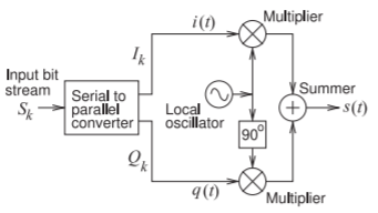
Figure \(\PageIndex{6}\): Quadrature modulator block diagram. An input bitstream, \(S_{k}\), is divided into two bitstreams, \(I_{k}\) and \(Q_{k}\), which are applied to the multipliers as (possibly filtered) waveforms \(i(t)\) and \(q(t)\). The output of the multipliers (appropriately filtered) are summed to yield a modulated carrier signal, \(s(t)\). The \(90^{\circ}\) block shifts the carrier by \(90^{\circ}\).
fortunate that the quadrature modulators can be implemented digitally followed possibly by wave-shaping. The differential signal \((m_{2}^{+}(t),\: m_{2}^{−}(t))\) is the phase-shifted form of \((m_{1}^{+}(t),\: m_{1}^{−}(t))\) in which every frequency component is shifted by \(90^{\circ}\) usually implemented as the Hilbert transform of the digital forms of \((m_{1}^{+}(t),\: m_{1}^{−}(t))\) (before wave-shaping).
Footnotes
[1] A duplexer separates transmitted and received signals and is often implemented as a filter called a diplexer. A diplexer separates two signals on different frequency bands so that they can use a common element such as an antenna. If the transmitted and received signals are in different time slots, the duplexer can be a switch.